- NXP Forums
- Product Forums
- General Purpose MicrocontrollersGeneral Purpose Microcontrollers
- i.MX Forumsi.MX Forums
- QorIQ Processing PlatformsQorIQ Processing Platforms
- Identification and SecurityIdentification and Security
- Power ManagementPower Management
- MCX Microcontrollers
- S32G
- S32K
- S32V
- MPC5xxx
- Other NXP Products
- Wireless Connectivity
- S12 / MagniV Microcontrollers
- Powertrain and Electrification Analog Drivers
- Sensors
- Vybrid Processors
- Digital Signal Controllers
- 8-bit Microcontrollers
- ColdFire/68K Microcontrollers and Processors
- PowerQUICC Processors
- OSBDM and TBDML
-
- Solution Forums
- Software Forums
- MCUXpresso Software and ToolsMCUXpresso Software and Tools
- CodeWarriorCodeWarrior
- MQX Software SolutionsMQX Software Solutions
- Model-Based Design Toolbox (MBDT)Model-Based Design Toolbox (MBDT)
- FreeMASTER
- eIQ Machine Learning Software
- Embedded Software and Tools Clinic
- S32 SDK
- S32 Design Studio
- Vigiles
- GUI Guider
- Zephyr Project
- Voice Technology
- Application Software Packs
- Secure Provisioning SDK (SPSDK)
- Processor Expert Software
-
- Topics
- Mobile Robotics - Drones and RoversMobile Robotics - Drones and Rovers
- NXP Training ContentNXP Training Content
- University ProgramsUniversity Programs
- Rapid IoT
- NXP Designs
- SafeAssure-Community
- OSS Security & Maintenance
- Using Our Community
-
-
- Home
- :
- General Purpose Microcontrollers
- :
- Kinetis Microcontrollers
- :
- K22F Debug Interface
K22F Debug Interface
- Subscribe to RSS Feed
- Mark Topic as New
- Mark Topic as Read
- Float this Topic for Current User
- Bookmark
- Subscribe
- Mute
- Printer Friendly Page
K22F Debug Interface
- Mark as New
- Bookmark
- Subscribe
- Mute
- Subscribe to RSS Feed
- Permalink
- Report Inappropriate Content
Hi, I would like to confirm the JTAG debug interface for MK22FN512VLH12.
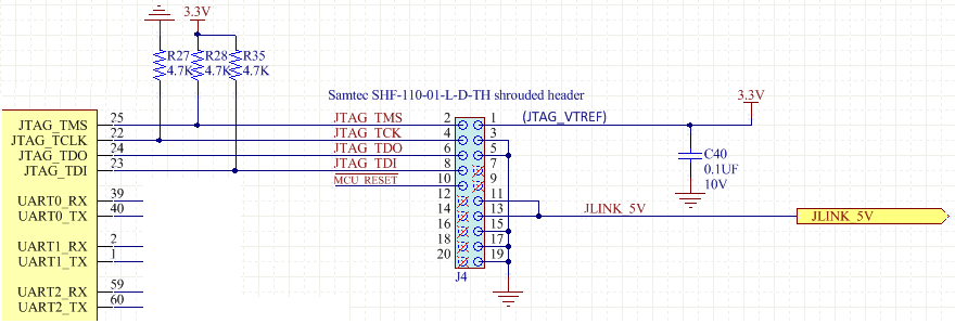
Following is a snippet of schematic that has worked in the past for K60-based controllers, but this is a new chip for us, so I want to make sure.
I verified with "Debug interface.pdf" which was kindly posted to this forum by Ping in August of this year (2015), but the document does not specify the strength of the pullup/down resistors, nor the direction, for all three pins in question.
Fortunately, the document does specify that pin 10 of the JTAG connector goes to the microcontroller main reset.
The 3.3V I think is used as reference for the JLink adapter, so it goes *out* of my PCB, whereas of course the pins 11 and 13 come *into* the PCB.
The MCU_RESET signal has a 10k pullup elsewhere in the schematic, not shown here.
Therefore, following questions:
- Can someone please confirm the usage of 3.3V, and also verify the below pullups/downs and pinouts are correct (for LQFP-64pin version)?
- Can someone please confirm I can feed a 50MHz clock (standalone MEMs oscillator, not resonator or crystal) into the EXTAL0 (pin 32) of this K22F device? The reference manual talks about 32MHz being the max, but I believe that is for a crystal; the FRDM board has the option of a 50MHz clock, and this oscillator has worked before for K60 designs.
- Can someone please point me to the Freedom board schematic for K22F? I found the hardware manual, etc., on the main page, but didn't see the schematic.
- Is there a "clean" reference design (not part of Freedom board) that does not use the SDA SWD stuff? This is where it becomes confusing a little.
- Is there a checklist for K22F designs?
Thank you very much
Michael
- Mark as New
- Bookmark
- Subscribe
- Mute
- Subscribe to RSS Feed
- Permalink
- Report Inappropriate Content
Hi Michael,
1> There is a document <Kinetis Peripheral Module Quick Reference> includes debug interface circuit design at chapter 2.1.5.3 (page 32) .
The pull up/down resistor application at the debugger interface circuit should be correct.
2> The K22 supports external 50MHz clock input as clock source at EXTAL0 pin.
3> Please download FRDM-K22F schematics from here.
4> Besides of <Kinetis Peripheral Module Quick Reference> document, customer could refer Kinetis Hardware design Tip& Tricks document from below link:
Kinetis Hardware Design Tip & Tricks
5> Unfortunately, there is no K22F checklist.
Wish it helps.
best regards,
Ma Hui
- Mark as New
- Bookmark
- Subscribe
- Mute
- Subscribe to RSS Feed
- Permalink
- Report Inappropriate Content
Thank you very much.
