
- NXP Forums
- Product Forums
- General Purpose MicrocontrollersGeneral Purpose Microcontrollers
- i.MX Forumsi.MX Forums
- QorIQ Processing PlatformsQorIQ Processing Platforms
- Identification and SecurityIdentification and Security
- Power ManagementPower Management
- MCX Microcontrollers
- S32G
- S32K
- S32V
- MPC5xxx
- Other NXP Products
- Wireless Connectivity
- S12 / MagniV Microcontrollers
- Powertrain and Electrification Analog Drivers
- Sensors
- Vybrid Processors
- Digital Signal Controllers
- 8-bit Microcontrollers
- ColdFire/68K Microcontrollers and Processors
- PowerQUICC Processors
- OSBDM and TBDML
-
- Solution Forums
- Software Forums
- MCUXpresso Software and ToolsMCUXpresso Software and Tools
- CodeWarriorCodeWarrior
- MQX Software SolutionsMQX Software Solutions
- Model-Based Design Toolbox (MBDT)Model-Based Design Toolbox (MBDT)
- FreeMASTER
- eIQ Machine Learning Software
- Embedded Software and Tools Clinic
- S32 SDK
- S32 Design Studio
- Vigiles
- GUI Guider
- Zephyr Project
- Voice Technology
- Application Software Packs
- Secure Provisioning SDK (SPSDK)
- Processor Expert Software
-
- Topics
- Mobile Robotics - Drones and RoversMobile Robotics - Drones and Rovers
- NXP Training ContentNXP Training Content
- University ProgramsUniversity Programs
- Rapid IoT
- NXP Designs
- SafeAssure-Community
- OSS Security & Maintenance
- Using Our Community
-
-
- Home
- :
- General Purpose Microcontrollers
- :
- Kinetis Microcontrollers
- :
- K60 ADC damage despite input protection
K60 ADC damage despite input protection
- Subscribe to RSS Feed
- Mark Topic as New
- Mark Topic as Read
- Float this Topic for Current User
- Bookmark
- Subscribe
- Mute
- Printer Friendly Page
K60 ADC damage despite input protection
- Mark as New
- Bookmark
- Subscribe
- Mute
- Subscribe to RSS Feed
- Permalink
- Report Inappropriate Content
We see ADC failures on meanwhile the third unit with a K60 (MK60DN512VLQ10 - 4N22D) from different pcb lots. They return gross stepping values from a linear voltage ramp on the input. There are no failures (yet) reported by the customer, the problems all appeared during software development.
The board already underwent overload tests on the inputs of -24 to +48V and full EMI testing (4kV burst and 30kV ESD) without failure.
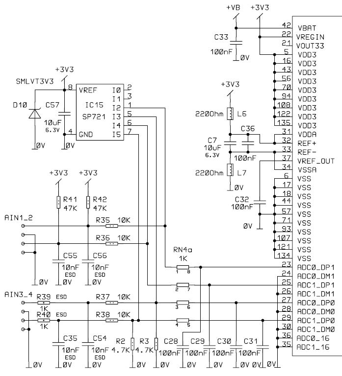
We are using the ADC0 & 1 inputs ADCx_DPx for measuring 0..10V (AIN3..4 in our schematic) and 10..100kOhms resistance (AIN 1..2) and the K60 temperature sensor.
The ADCs are set to 6,25MHz, 16 bits, DIFF, Vref=3.3V, AV=32.
DAC0 drives a 4..20mA output circuit and continues to work correctly on the faulty boards.
Faulty stepping response from a ascending input signal (ADC Mode for this Test: 16Bit, DIFF=Off, REF=ALT)

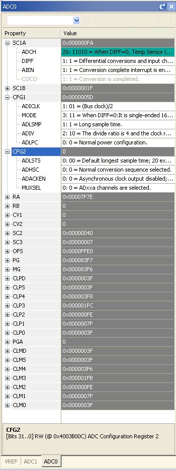
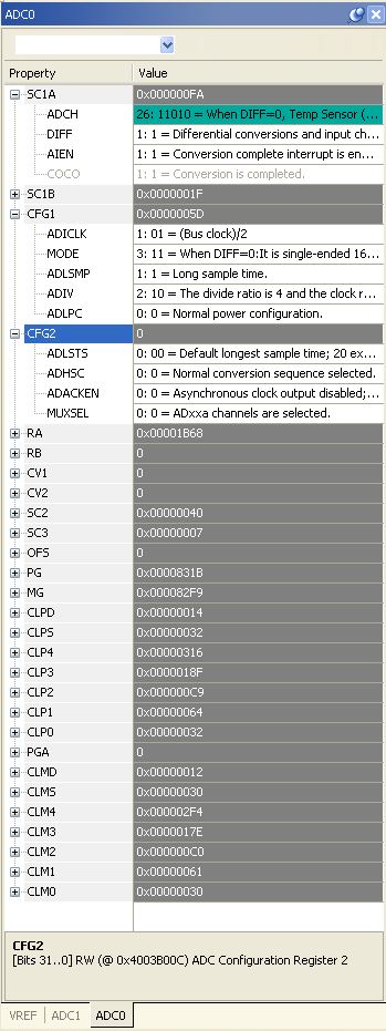
Differences in register states (Temp Sensor, 16Bit, Diff, REF=3.3V) ("K60ADC-good-registers.jpg" and "K60ADC-faulty-registers.jpg")
ADC part of the schematic ("K60ADC-schematic.jpg")
In our overload tests we have seen the following currents and voltages which all should not lead to a circuit damage.
U_AIN3_4: -24V (20x 1s):
------------------
U_SP721: -0,69V
UinADC0_DP1: -0,561V
IinADC0_DP1: -130uA
U_AIN3_4: +48V (20x 1s):
-------------------
U_SP721: +4,08V
UinADC0_DP1: +4,00V
IinADC0_DP1: +80uA
U_AIN1_2: ESD Contact +/-2KV (20x) : OK
U_AIN3_4: ESD Contact +/-2KV (20x) : OK
Hence we have no idea where the faults have there origin. Any ideas?
Thanks.
Mike
- Mark as New
- Bookmark
- Subscribe
- Mute
- Subscribe to RSS Feed
- Permalink
- Report Inappropriate Content
Mike, I know this ADC problem happened years ago, but I now have exactly the same problem on a K66 and wanted to know if you ever found a root cause. In my application, I run one ADC channel (on adc0) in single-ended mode at the maximum continuous speed for 16-bit. Then, I stop acquisition, and restart it frequently (eg 30Hz) since data is acquired sporadically. After 3-5 days of correct operation, the ADC always fails spontaneously in the same way: it still produces a result, but the digital codes do not correspond exactly with the analog value. I attached a test waveform, which should be a smooth sawtooth. I've added protection diodes, higher value resistors on the inputs, changed grounding methods, and cannot understand why the chip dies. Let me know if you ever learned anything about this. Thanks!

- Mark as New
- Bookmark
- Subscribe
- Mute
- Subscribe to RSS Feed
- Permalink
- Report Inappropriate Content
Hello Ben,
we have no more Fails (Kinetis CPU's with damaged ADCs), since we limit the max. Input Voltage to <3,2V. (Clamping Diodes now to 2,5V). Are your ADCs also damaged like ours (no more correct Function after power on) ?
Mike
- Mark as New
- Bookmark
- Subscribe
- Mute
- Subscribe to RSS Feed
- Permalink
- Report Inappropriate Content
Mike, thanks so much for your quick reply. Yes, in my case, the adc is permanently damaged, and switching to a different pin on the same adc doesn't help. It's interesting that your solution of clamping to 2.5V worked -- maybe these chips are incredibly sensitive to overvoltage transients. I'll have to give that a try.
- Mark as New
- Bookmark
- Subscribe
- Mute
- Subscribe to RSS Feed
- Permalink
- Report Inappropriate Content
The input protection looks good. The only thing I see that I don't like with the circuit is L7 - but I think that would just add noise to your readings. It seems unlikely that it would create negative voltage spikes on REF- / VSSA low enough to damage the part. I am not sure why someone designed in L7, it defeats the purpose of L6 and C7 / C36.
The more I look at the filtering on the analog voltage the less I like it. I don't know on the K60, but many parts want the VSSA to be very close to VSS, +/-100ms. If your 3.3V slews up and down at a fast rate, then the large C7 with L7 could cause problems with VSSA. Do the software development boards get a lot more power cycles than the field units? You could try cycling power a few hundred times to see if that will force the problem. Consider shorting L7 and reducing C7.
- Mark as New
- Bookmark
- Subscribe
- Mute
- Subscribe to RSS Feed
- Permalink
- Report Inappropriate Content
Chip,
L7 and L6 are BLM18SG221TN1 SMT-ferrites. The filter circuit is a modified/reduced version of the TWR-K60N512 filter.
Do you mean, the 10uF C7 cause more REF-/ VSSA stress ?
Our first unit with the most power cycles and I/O- und JTAG- connections/disconnections works without any problems. But for this unit we are using an other JTAG/SWI programmer (ULINK-ME (USB powered) instead OSBM (board powered)).
Mike
- Mark as New
- Bookmark
- Subscribe
- Mute
- Subscribe to RSS Feed
- Permalink
- Report Inappropriate Content
At 100 MHz L6 and L7 appear to look mostly resistive, at about 220 Ohms. With your 10 uF cap, this is a time constant of 4.4 ms, indicating over a 100 MHz noise spike the cap will remain stable. If a positive spike of say 100 mV comes in on 3.3V, then the VDDA and VSSA will both rise by 50 mV, with 50 mV being seen across both L6 and L7. Shorting the bottom inductor / bead will keep the noise spike off of VDDA and VSSA, with the full noise spike appearing across L6.
My larger concern is if when voltage is applied to the device, with the 10 uF cap at 0V, the rising edge will be shared across the L6 and L7. (Looking at the TWR schematic, they used a 0.1 uF instead of teh 10 uF, which will reduce the problem.) The K60 datasheet requires VDDA to be within +/- 100 mV of VDD and VSSA to be within +/- 100 mV of VSS. If you have a fast rise time on your power supply, or a fast decay time, then this spec could be violated. By reducing the 10 uF to 0.1 uF you will allow 100x the rise time. Maybe one of the Freescale engineers could comment on if the +/- 100 mV violation will cause damage to the part (my guess is that it can).
You may want to look at the power supply rise and fall times of your first unit, and the units which have failed. If they are much faster, that could explain the problem.
- Mark as New
- Bookmark
- Subscribe
- Mute
- Subscribe to RSS Feed
- Permalink
- Report Inappropriate Content
Thank you for commenting again on my problem! Following your advice, I tried to test and simulate over- and undershoots on the reference. In LTSPICE it would indeed result in 0.6V (30mV without the 10uF) excursions from a full step VCC change in a few microseconds. In reality, I couldn't produce more than 200mV changes. So next I applied short pulses (less than a second) of 1V (up to 1A) positive and negative at Ref-/Vssa Pin (to force a fail).The ADC values would be affected during these pulses but the ADC returned to proper operation despite many such cycles.
Hence, while we will definitely follow your advice and short L7 while reducing C7 to 10nF, we don't think that this really solves the problem. One of the reasons to be doubtful is that on the first failing unit it was one channel only that failed in the beginning. Though the other followed later, this speaks against a Vref cause. Any other idea?
Mike