- NXP Forums
- Product Forums
- General Purpose MicrocontrollersGeneral Purpose Microcontrollers
- i.MX Forumsi.MX Forums
- QorIQ Processing PlatformsQorIQ Processing Platforms
- Identification and SecurityIdentification and Security
- Power ManagementPower Management
- MCX Microcontrollers
- S32G
- S32K
- S32V
- MPC5xxx
- Other NXP Products
- Wireless Connectivity
- S12 / MagniV Microcontrollers
- Powertrain and Electrification Analog Drivers
- Sensors
- Vybrid Processors
- Digital Signal Controllers
- 8-bit Microcontrollers
- ColdFire/68K Microcontrollers and Processors
- PowerQUICC Processors
- OSBDM and TBDML
-
- Solution Forums
- Software Forums
- MCUXpresso Software and ToolsMCUXpresso Software and Tools
- CodeWarriorCodeWarrior
- MQX Software SolutionsMQX Software Solutions
- Model-Based Design Toolbox (MBDT)Model-Based Design Toolbox (MBDT)
- FreeMASTER
- eIQ Machine Learning Software
- Embedded Software and Tools Clinic
- S32 SDK
- S32 Design Studio
- Vigiles
- GUI Guider
- Zephyr Project
- Voice Technology
- Application Software Packs
- Secure Provisioning SDK (SPSDK)
- Processor Expert Software
-
- Topics
- Mobile Robotics - Drones and RoversMobile Robotics - Drones and Rovers
- NXP Training ContentNXP Training Content
- University ProgramsUniversity Programs
- Rapid IoT
- NXP Designs
- SafeAssure-Community
- OSS Security & Maintenance
- Using Our Community
-
-
- Home
- :
- General Purpose Microcontrollers
- :
- Kinetis Microcontrollers
- :
- Using DMA to Emulate ADC Flexible Scan Mode on Kinetis K Series
Using DMA to Emulate ADC Flexible Scan Mode on Kinetis K Series
- Subscribe to RSS Feed
- Mark Topic as New
- Mark Topic as Read
- Float this Topic for Current User
- Bookmark
- Subscribe
- Mute
- Printer Friendly Page
Using DMA to Emulate ADC Flexible Scan Mode on Kinetis K Series
- Mark as New
- Bookmark
- Subscribe
- Mute
- Subscribe to RSS Feed
- Permalink
- Report Inappropriate Content
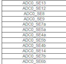
I use the following ADC0 channel:
ADC0_SE13 |
ADC0_SE12 |
ADC0_SE8 |
ADC0_SE9 |
ADC0_SE7a |
ADC0_SE5a |
ADC0_SE4a |
ADC0_SE5b |
ADC0_SE4b |
ADC0_SE14 |
ADC0_SE7b |
ADC0_SE6b |
ADCx_SEn channels a and b have different ADCx_CFG2[MUXSEL] bit, how can I still Use DMA to Emulate ADC Flexible Scan Mode on Kinetis K Series?
Do I need to set 3 DMA channel?
If DMA mode still works well, can you show me detail process flow?
- Mark as New
- Bookmark
- Subscribe
- Mute
- Subscribe to RSS Feed
- Permalink
- Report Inappropriate Content
Hi Linjie Pan,
The eDMA in Kinetis K family supports minor loop and major loop, so after you start an ADC conversion, COCO bit will fire an ADC0 interrupt, which issues an eDMA minor loop if you enable ADC DMA function, then you may configure ADCx_SC1n and ADCx_CFG2 in each minor loop, and may repeat the ADC sample sequence when eDMA interrupt happens after major loop done.
For this process, just one DMA channel is needed, but if you use a linked channel to configure ADCx_CFG2 on minor-loop complete , then you have to use 2 channels.
BTW, for ADC_SE12 and something like that, ADCx_CFG2[MUXSEL] bit has no meaning, so you may set it as default value of zero.
Hope that makes sense,
Please kindly let me know if you have any issue,
Have a great day,
Kan
Freescale Technical Support
-----------------------------------------------------------------------------------------------------------------------
Note: If this post answers your question, please click the Correct Answer button. Thank you!
-----------------------------------------------------------------------------------------------------------------------
- Mark as New
- Bookmark
- Subscribe
- Mute
- Subscribe to RSS Feed
- Permalink
- Report Inappropriate Content
Hi, Kan:
When I read the code about 'DMA channel initlization'. I met with an issue :
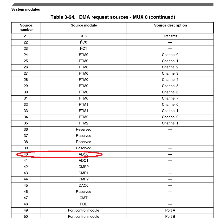
One configuration is " DMAMUX_CHCFG1 = DMAMUX _CHCFG_ENBL|DMAMUX_CHCFG_SOURCE(40) ". Could you tell me what does this "40" mean?
I've checked the detailed information about 'Channel Configuration Register (DMAMUX_CHCFGn)' in the K10 Chip manual.
The DMAMUX_CHCFG[SOURCE] represents " DMA Channel Source (slot) ". It's described as " Specifies which DMA source, if any, is routed to a particular DMA channel. Please check your device's Chip Configuration details for further details about the peripherals and their slot numbers."
The " slot numbers" (such as 40) correspond to what DMA source, could you tell me?
PS: the chip I used is K10 series.
- Mark as New
- Bookmark
- Subscribe
- Mute
- Subscribe to RSS Feed
- Permalink
- Report Inappropriate Content
Hi Yanli Cheng,
If you refer to Chapter 3 Chip Configuration in K10P100M100SF2V2RM.pdf, you may find details regarding DMA source on page 85, and 40 here represents ADC0, please refer to the following for more details.
Hope that helps,
Have a great day,
Kan
Freescale Technical Support
-----------------------------------------------------------------------------------------------------------------------
Note: If this post answers your question, please click the Correct Answer button. Thank you!
-----------------------------------------------------------------------------------------------------------------------
- Mark as New
- Bookmark
- Subscribe
- Mute
- Subscribe to RSS Feed
- Permalink
- Report Inappropriate Content
Thanks a lot for your answer, Kan_Li. I've found this table in the chip manual under your help.
But I'm still confused about the concept of 'DMA request source'. I've tried to search some useful explanations on the web, but still not found anything clear.
Could you help to explain or give some useful reference?
My confustion can be illustrated by the following 2 examples:
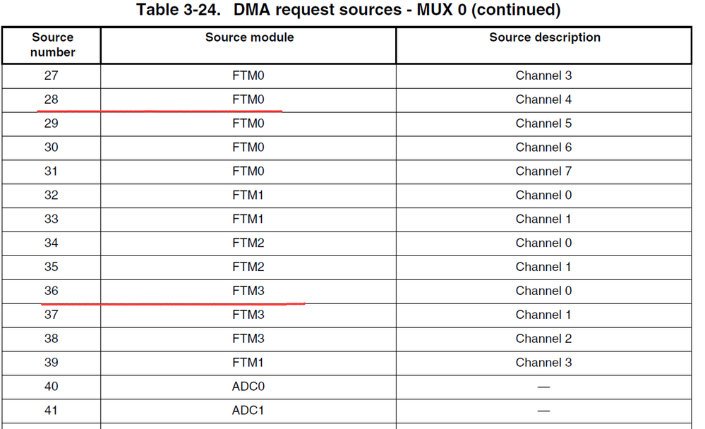
(1) I want to use DMA to transfer ADC data and I refer to the document "Using DMA to Emulate ADC Flexible Scan Mode on Kinetis K Series", which is downloaded from FreeScale official website. In the 'DMA channel Initialization' part, the DMA channel 1 request source was configured as "DMAMUX_CHCFG1 = DMAMUX _CHCFG_ENBL|DMAMUX_CHCFG_SOURCE(28); " , and DMA channel 0 request source was configured as "DMAMUX_CHCFG0 = DMAMUX _CHCFG_ENBL|DMAMUX_CHCFG_SOURCE(36) ; " . This example uses the Freescale TRW-K60N512 development board. I checked the K60 chip reference manual and knowed that '28' represents FTM0 and '40' represents FTM3.
(2) When I do research about another project example, which use K10 series chip and also use DMA to transfer ADC data. The DMA channel 1 and channel 0 request source are all configured as '40'. According to the K10 reference manual , this means DMA channel1 and channel 0 request source are all 'ADC0 '. Other configurations are similar to example one.
In a word, how to configured the DMA request source? Based on what principle?
- Mark as New
- Bookmark
- Subscribe
- Mute
- Subscribe to RSS Feed
- Permalink
- Report Inappropriate Content
Hi Yanli Cheng,
Actually you may understand eDMA module as a co-processor for MCU, the DMA channles are interrupts of this co-processor, and DMA sources are just like interrupt sources, but more flexible , for example, the same DMA sources can be assigned to different DMA channels, but it is not recommended sharing one source for different channels , because RM says "Setting multiple CHCFG registers with the same Source value will result in unpredictable behavior."
and when you assign some source to a DMA channel, this module will have the trigger signal from that source under some condition , for example, if the DMA source is ADC0, the trigger signal comes when ADC0 COCO bit is set, and then DMA module does the presetting transfer just like a co-process handles the ISR.
so you may assign to any DMA channel with any DMA source, depending on your application.
For more details on DMA source, you may refer to the chapters in RM, each module which has DMA support usually has a register regarding DMA operation, which can be found under the section of "Register definition". and some module chapter contains a section for DMA operation as well, such as FTM module.
Hope that helps,
Have a great day,
Kan
Freescale Technical Support
-----------------------------------------------------------------------------------------------------------------------
Note: If this post answers your question, please click the Correct Answer button. Thank you!
-----------------------------------------------------------------------------------------------------------------------
- Mark as New
- Bookmark
- Subscribe
- Mute
- Subscribe to RSS Feed
- Permalink
- Report Inappropriate Content
Hi, Kan_Li:
I want to ask you a question. As to freescale K10 chip, is there a default priority setting among the 16 DMA channels?
That means ,does channel (n+x) has a higher priority than channel n ?
Because in the pdf document " Using DMA to Emulate ADC Flexible Scan Mode on Kinetis K Series", it says :
I didn't find corresponding information about default priority in the RM(only finds the register 'DMA_DCHPRIn' can set priority for DMA channel n).
- Mark as New
- Bookmark
- Subscribe
- Mute
- Subscribe to RSS Feed
- Permalink
- Report Inappropriate Content
Hi Yanli Cheng,
Actually eDMA supports fixed-priority and round-robin channel arbitration, which is controlled by DMA_CR[ERCA], and module uses fixed-priority arbitration out of reset, in which the channel service request from the highest priority channel is selected to execute, and the contents of DMA_DCHPRIn defines the unique priorities associated with each channel . The channel priorities are evaluated by numeric value; for example, 0 is the lowest priority, 1 is the next priority, then 2, 3, etc. Software must program the channel priorities with unique values;otherwise, a configuration error is reported.
and for round-robin arbitration, channels are serviced starting with the highest channel number and rotating through to the lowest channel number without regard to the channel priority levels.
Hope that makes sense,
Have a great day,
Kan
Freescale Technical Support
-----------------------------------------------------------------------------------------------------------------------
Note: If this post answers your question, please click the Correct Answer button. Thank you!
-----------------------------------------------------------------------------------------------------------------------
- Mark as New
- Bookmark
- Subscribe
- Mute
- Subscribe to RSS Feed
- Permalink
- Report Inappropriate Content
Thanks, Kan_Li.
According to your explanation above and the information in RM, can I understand it in the following way?
There are several DMA channels and each channel has its own service request. If I don't configure DMA_CR, the module uses fixed-priority arbitration (in a default way because of reset). I must program the channel priorities by the register ' DMA_DCHPRIn' ; otherwise, a configuration error is reported.
In another situation, if I arrange 3 DMA channels: channel 1 links to channel 0, and channel 0 links to channel 3 (All done by configuring the 'DMA_CSR_MAJORLINKCH' ).
Then even I don't set 'DMA_CR' and 'DMA_DCHPRIn' , will the service request of channel 1 be done first , then channel 0 ,and last channel 3?
- Mark as New
- Bookmark
- Subscribe
- Mute
- Subscribe to RSS Feed
- Permalink
- Report Inappropriate Content
Hi Yanli Cheng,
You don't need to program ' DMA_DCHPRIn' out of reset, because Reset value for the channel priority fields, CHPRI, is equal to the corresponding channel number
for each priority register, i.e., DCHPRI15[CHPRI] equals 0b1111.
For your second question, my answer is yes.
Hope that helps,
Please kindly let me know if you have any further question.
Have a great day,
Kan
Freescale Technical Support
-----------------------------------------------------------------------------------------------------------------------
Note: If this post answers your question, please click the Correct Answer button. Thank you!
-----------------------------------------------------------------------------------------------------------------------
- Mark as New
- Bookmark
- Subscribe
- Mute
- Subscribe to RSS Feed
- Permalink
- Report Inappropriate Content
Hi, Kan_Li:
We discussed about the issue stated at the top of this page: using an extra DMA channel 3 so as to choose between 'a' channel and 'b' channel (such as 'ADC0_SE5a' and 'ADC0_SE5b') . When I tried to apply it, I met with a problem and were confused. Hope you can give me some clue.
【Problem Description】
I initiate DMA channel 0,1 and 3, referring to the freescale official document "Use DMA to Emulate ADC Flexible Scan Mode on Kinetis K Series".
(1)DMA channel 1 was used to transfer ADC result from 'ADC0_RA' to buffer 'dma_adc_buff'. Major loop transfers number 16*12.
(2)DMA channel 0 was used to choose the next ADC channel number. Major loop transfers number 12.
(3)DMA channel 3 was used to choose 'MUXSEL_ADCA' or 'MUXSEL_ADCB' for the next channel. Major loop transfers number 12.
Source address and destination address are separately set as follows:
| DMA_TCD3_SADDR = (uint32)&channel_muxsel_map[0]; | |
| DMA_TCD3_DADDR = (uint32)&ADC0_CFG2; |
The channel_muxsel_map[12] is an array, storing the 'MUXSEL_ADCA' or 'MUXSEL_ADCB' message for each ADC channel.
In the test, the ADC channel number is selected in a right order. However, the 'a' or 'b' selection work in disorder.
Would you know what may cause this to happen?
- Mark as New
- Bookmark
- Subscribe
- Mute
- Subscribe to RSS Feed
- Permalink
- Report Inappropriate Content
Hi Yanli Cheng,
Per your application, I would recommend you using one channel for two DMA transfer you mentioned above:
(2)DMA channel 0 was used to choose the next ADC channel number. Major loop transfers number 12.
(3)DMA channel 3 was used to choose 'MUXSEL_ADCA' or 'MUXSEL_ADCB' for the next channel. Major loop transfers number 12.
you may find the above two have the same Major loop transfers. so you may do them both in a single channel. for example, channel 0.
so channel 1 used to move the ADC results, channel 0 used to configure the registers of ADCx_SC1A and ADCx_CFG2.
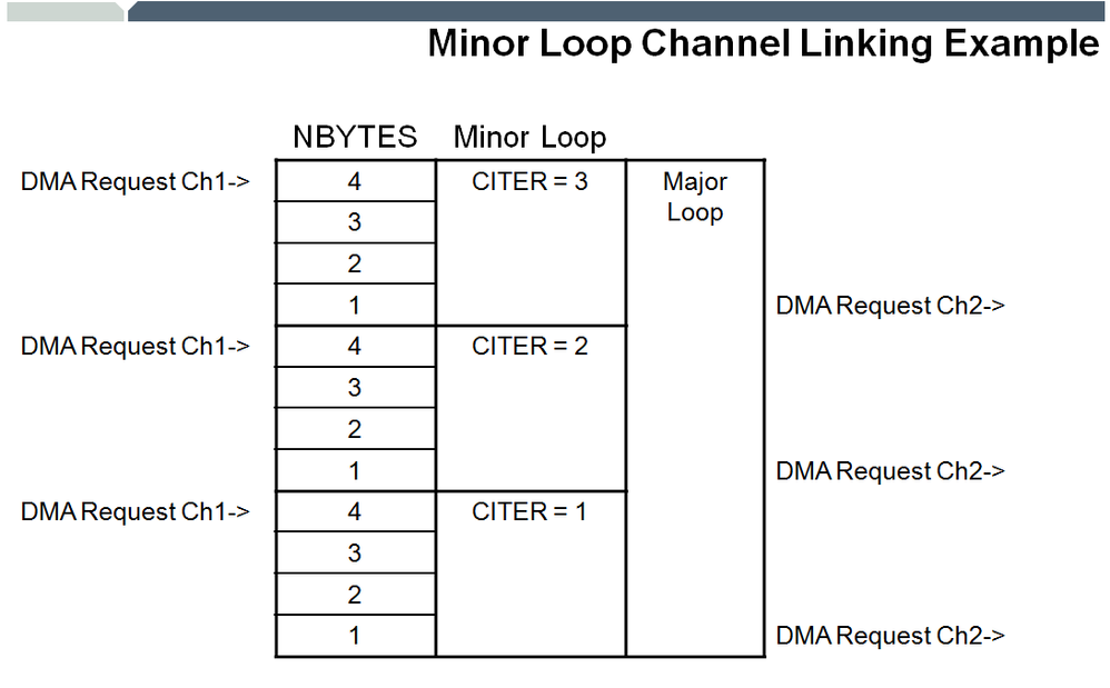
Please enable Minor Loop Channel Linking mode for that case. ADC0 COCO triggers Channel 1 transfer, and each minor loop completion event trigger channel 0 transfer. Please refer to the following for more details.
Hope that helps,
Have a great day,
Kan
Freescale Technical Support
-----------------------------------------------------------------------------------------------------------------------
Note: If this post answers your question, please click the Correct Answer button. Thank you!
-----------------------------------------------------------------------------------------------------------------------
- Mark as New
- Bookmark
- Subscribe
- Mute
- Subscribe to RSS Feed
- Permalink
- Report Inappropriate Content
Thanks so much, Kan_Li. Your answer helps me a lot.
(1) I rechecked my code according to your answer, and found one mistake: although I enable 'Minor Loop Channel Linking', I didn't set the linking channel number ( I only set it in 'Major Loop Channel Linking'). In old project, because DMA channel 1 links to channel 0, it doesn't matter whether DMA_BITER_ELINKYES_LINKCH(x) is set. But in my new project when DMA channel 0 links to channel 3, I must set this value.
(2) I still use 3 DMA channels, and it can work. Now the 'MUXSEL_ADCA' or 'MUXSEL_ADCB' selection works right.
In your answer, you recommend that I use DMA 0 to to configure the registers of ADCx_SC1A and ADCx_CFG2. I don't understand how to realize it. The destination address can only be set to the address of one register, right? How to simultaneously use both ADCx_SC1A and ADCx_CFG2 as the destination address?
When I initiate DMA channel 0, I set :
DMA_TCD0_SADDR = (uint32)&channel_map[0];
DMA_TCD0_DADDR = (uint32)&ADC0_SC1A;
- Mark as New
- Bookmark
- Subscribe
- Mute
- Subscribe to RSS Feed
- Permalink
- Report Inappropriate Content
Hi Yanli Cheng,
You may use DMA_TCDn_ATTR[DMOD] to set a circular buffer for ADCx_SC1A and ADCx_CFG2.
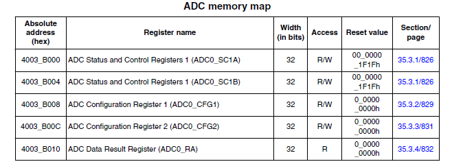
Per above, ADC0_SC1A is at 0x4003b000, and ADC0_CFG2 is at 0x4003b00c, so you may set a 16 bytes circular buffer for them. please note if you do in that way, ADC0_SC1B and ADC0_CFG1 are also included in this buffer, you have to prepare data for them as well. for more details regarding modulo, please refer to 22.5.4.3 Using the modulo feature.
Hope that helps,
Have a great day,
Kan
Freescale Technical Support
-----------------------------------------------------------------------------------------------------------------------
Note: If this post answers your question, please click the Correct Answer button. Thank you!
-----------------------------------------------------------------------------------------------------------------------
- Mark as New
- Bookmark
- Subscribe
- Mute
- Subscribe to RSS Feed
- Permalink
- Report Inappropriate Content
Hi, Kan_Li:
In the RM for K10 series chip, the 'PDBx_MOD' register was described as follows:
When I study one project, the setting for PDB is: PDB0_MOD = 50000000/(samplerate*4);
Here, samplerate=2000, and thus PDB0_MOD =6250.
I've two questions.
(1) In my view, 50000000 is the frequency of bus clock. and also the counter frequency of PDB. Is that right?
(2) When I changed 'PDB0_MOD' to a smaller value, such as 5000. The program will reset. What causes this to happen?
- Mark as New
- Bookmark
- Subscribe
- Mute
- Subscribe to RSS Feed
- Permalink
- Report Inappropriate Content
Okay, thanks a lot.
- Mark as New
- Bookmark
- Subscribe
- Mute
- Subscribe to RSS Feed
- Permalink
- Report Inappropriate Content
Got it. Thanks a lot!
- Mark as New
- Bookmark
- Subscribe
- Mute
- Subscribe to RSS Feed
- Permalink
- Report Inappropriate Content
Thank you for your professional reply. I have a better understanding of this concept after reading your answer, I'll refer to the RM further for more details.
Best regards!
