- NXP Forums
- Product Forums
- General Purpose MicrocontrollersGeneral Purpose Microcontrollers
- i.MX Forumsi.MX Forums
- QorIQ Processing PlatformsQorIQ Processing Platforms
- Identification and SecurityIdentification and Security
- Power ManagementPower Management
- MCX Microcontrollers
- S32G
- S32K
- S32V
- MPC5xxx
- Other NXP Products
- Wireless Connectivity
- S12 / MagniV Microcontrollers
- Powertrain and Electrification Analog Drivers
- Sensors
- Vybrid Processors
- Digital Signal Controllers
- 8-bit Microcontrollers
- ColdFire/68K Microcontrollers and Processors
- PowerQUICC Processors
- OSBDM and TBDML
-
- Solution Forums
- Software Forums
- MCUXpresso Software and ToolsMCUXpresso Software and Tools
- CodeWarriorCodeWarrior
- MQX Software SolutionsMQX Software Solutions
- Model-Based Design Toolbox (MBDT)Model-Based Design Toolbox (MBDT)
- FreeMASTER
- eIQ Machine Learning Software
- Embedded Software and Tools Clinic
- S32 SDK
- S32 Design Studio
- Vigiles
- GUI Guider
- Zephyr Project
- Voice Technology
- Application Software Packs
- Secure Provisioning SDK (SPSDK)
- Processor Expert Software
-
- Topics
- Mobile Robotics - Drones and RoversMobile Robotics - Drones and Rovers
- NXP Training ContentNXP Training Content
- University ProgramsUniversity Programs
- Rapid IoT
- NXP Designs
- SafeAssure-Community
- OSS Security & Maintenance
- Using Our Community
-
-
- Home
- :
- General Purpose Microcontrollers
- :
- Kinetis Microcontrollers
- :
- KL15 Locked - Bootloader Development - Need Help
KL15 Locked - Bootloader Development - Need Help
- Subscribe to RSS Feed
- Mark Topic as New
- Mark Topic as Read
- Float this Topic for Current User
- Bookmark
- Subscribe
- Mute
- Printer Friendly Page
KL15 Locked - Bootloader Development - Need Help
- Mark as New
- Bookmark
- Subscribe
- Mute
- Subscribe to RSS Feed
- Permalink
- Report Inappropriate Content
Hello,
I was working with another FWE, and we have seems to 'bricked' our KL15, which working on our custom bootloader. We're looking to figure out a method of unlocking the device.
Here are some details:
- Using Processor Expert v10.4, and adding a flash_LDD component and configured more or less standard with adding a new extra functions from the methods options
- Exporting PE Project to Keil.
- During an attempted write and restart, the device has no SWD Communication.
- Using the JLINK Cmd Prompt, the SWD is not available: **See Attached Pic: 'unnamed.jpg"
- Attempting to hold reset down while writing the device I get this message in Keil: **See attached Pic: "Keil.jpg"
Any idea what happened? Did we overwrite a special place in flash?
Is this chip toast?
Here are some other details from the other FWE:
"I was working on adding a small region above the flash configuration section .cfmconfig in the scatter file to contain app version info at fixed location. The location was 0x410 (flash config at 0x400) and I moved the .text region up by 0x40 bytes to make room for the new region which was mostly a copy of this:"
#define FlashConfig_size 0x00000010
...
ER_FlashConfig FlashConfig_start FlashConfig_size { ; load address = execution address
.ANY (.cfmconfig)
}
}
Please help us if you can thanks,
-Peter
- Mark as New
- Bookmark
- Subscribe
- Mute
- Subscribe to RSS Feed
- Permalink
- Report Inappropriate Content
Hi Peter,
Could you provides KL15 Flash configuration field value?
And if it is possible, could you provide the KL15 SWD interface related circuit also?
Thank you for the attention.
Have a great day,
Ma Hui
-----------------------------------------------------------------------------------------------------------------------
Note: If this post answers your question, please click the Correct Answer button. Thank you!
-----------------------------------------------------------------------------------------------------------------------
- Mark as New
- Bookmark
- Subscribe
- Mute
- Subscribe to RSS Feed
- Permalink
- Report Inappropriate Content
Hello Ma Hui,
For SWD:
- Using JLINK Base, 1.8V logic, See Attached picture.
- nRst jump is populated, and no pullups or pulldowns are on.
- System worked flawlessly before we started working with the flash and killed it.
For Flash Config:
-I am sorry but I will need some guidance on how to find those things. We use PE (Driver Suite 10.4) to export into Keil, and then this project has it's specific settings.
- **See 2nd picture attached, is this what you wanted? If not please send more detail to I can get you what you need.
Thanks Mu Hui,
-Peter
- Mark as New
- Bookmark
- Subscribe
- Mute
- Subscribe to RSS Feed
- Permalink
- Report Inappropriate Content
Hi,
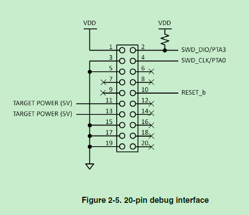
1. About SWD interface, your attached SWD debug interface is different with Freescale recommended at pin numbers order.
For you could program and debug the KL15 chip before, I think that's ok.
Below is Freescale recommended SWD debug interface:
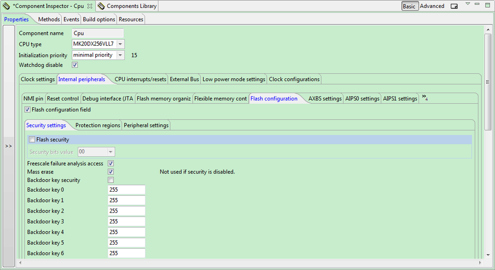
2. For you are using the Processor Expert v10.4, I would you could provide the Flash configuration field value.
Please check below picture as a reference:
Thank you for the attention.
Have a great day,
Ma Hui
-----------------------------------------------------------------------------------------------------------------------
Note: If this post answers your question, please click the Correct Answer button. Thank you!
-----------------------------------------------------------------------------------------------------------------------

