- NXP Forums
- Product Forums
- General Purpose MicrocontrollersGeneral Purpose Microcontrollers
- i.MX Forumsi.MX Forums
- QorIQ Processing PlatformsQorIQ Processing Platforms
- Identification and SecurityIdentification and Security
- Power ManagementPower Management
- MCX Microcontrollers
- S32G
- S32K
- S32V
- MPC5xxx
- Other NXP Products
- Wireless Connectivity
- S12 / MagniV Microcontrollers
- Powertrain and Electrification Analog Drivers
- Sensors
- Vybrid Processors
- Digital Signal Controllers
- 8-bit Microcontrollers
- ColdFire/68K Microcontrollers and Processors
- PowerQUICC Processors
- OSBDM and TBDML
-
- Solution Forums
- Software Forums
- MCUXpresso Software and ToolsMCUXpresso Software and Tools
- CodeWarriorCodeWarrior
- MQX Software SolutionsMQX Software Solutions
- Model-Based Design Toolbox (MBDT)Model-Based Design Toolbox (MBDT)
- FreeMASTER
- eIQ Machine Learning Software
- Embedded Software and Tools Clinic
- S32 SDK
- S32 Design Studio
- Vigiles
- GUI Guider
- Zephyr Project
- Voice Technology
- Application Software Packs
- Secure Provisioning SDK (SPSDK)
- Processor Expert Software
-
- Topics
- Mobile Robotics - Drones and RoversMobile Robotics - Drones and Rovers
- NXP Training ContentNXP Training Content
- University ProgramsUniversity Programs
- Rapid IoT
- NXP Designs
- SafeAssure-Community
- OSS Security & Maintenance
- Using Our Community
-
-
- Home
- :
- General Purpose Microcontrollers
- :
- Kinetis Microcontrollers
- :
- Connecting K60D100m to External flash using flex bus interface
Connecting K60D100m to External flash using flex bus interface
- Subscribe to RSS Feed
- Mark Topic as New
- Mark Topic as Read
- Float this Topic for Current User
- Bookmark
- Subscribe
- Mute
- Printer Friendly Page
Connecting K60D100m to External flash using flex bus interface
- Mark as New
- Bookmark
- Subscribe
- Mute
- Subscribe to RSS Feed
- Permalink
- Report Inappropriate Content
Hi,
We are working on K60 evalution board to connect to micron external flash (M29W128GL) , using flex bus configuration (16 bit address and 16 bit data) in multiplexed mode. We have taken care of AD0 pin which is used only for data and not for address.
We are following example code of flexbus given by freescale.
IDE : IAR embedded workbench
please let me know if we are missing anything from the initialization code.
Even we are using micron flash drivers for flash init and checking comapatability but not getting right values.
void TWRK60_flexbus_init(void)
{
/* Enable the FlexBus */
/* Configure the FlexBus Registers for 8-bit port size */
/* with separate address and data using chip select 0 */
/* These configurations are specific to communicating with */
/* the MRAM used in this example */
/* For K60 tower module - do not set byte lane shift so that data */
/* comes out on AD[31:24] */
//Set Base address
FB_CSAR0 = (uint32)&MRAM_START_ADDRESS; //0x60000000
FB_CSCR0 = FB_CSCR_PS(1) // 8-bit port - Changed to FB_CSCR_PS(2) // 16 bit port
| FB_CSCR_AA_MASK // auto-acknowledge
| FB_CSCR_ASET(0x1) // assert chip select on second clock edge after address is asserted
| FB_CSCR_WS(0x2) // 1 wait state - may need a wait state depending on the bus speed
;
FB_CSCR0 |= FB_CSCR_BLS_MASK ; Do we need to do this for k60??
FB_CSMR0 = FB_CSMR_BAM(0x7) //Set base address mask for 512K address space
| FB_CSMR_V_MASK //Enable cs signal
;
//enable BE signals - note, not used in this example
FB_CSPMCR = 0x02200000;
//fb clock divider 3
SIM_CLKDIV1 |= SIM_CLKDIV1_OUTDIV3(0x3); // tried changing this also
// Set the GPIO ports clocks
SIM_SCGC5 = SIM_SCGC5_PORTA_MASK | SIM_SCGC5_PORTB_MASK | SIM_SCGC5_PORTC_MASK |
SIM_SCGC5_PORTD_MASK | SIM_SCGC5_PORTE_MASK;
/* Configure the pins needed to FlexBus Function (Alt 5) */
/* this example uses low drive strength settings */
//address
PORTB_PCR11 = PORT_PCR_MUX(5); // fb_ad[18]
PORTB_PCR16 = PORT_PCR_MUX(5); // fb_ad[17]
PORTB_PCR17 = PORT_PCR_MUX(5); // fb_ad[16]
PORTB_PCR18 = PORT_PCR_MUX(5); // fb_ad[15]
PORTC_PCR0 = PORT_PCR_MUX(5); // fb_ad[14]
PORTC_PCR1 = PORT_PCR_MUX(5); // fb_ad[13]
PORTC_PCR2 = PORT_PCR_MUX(5); // fb_ad[12]
PORTC_PCR4 = PORT_PCR_MUX(5); // fb_ad[11]
PORTC_PCR5 = PORT_PCR_MUX(5); // fb_ad[10]
PORTC_PCR6 = PORT_PCR_MUX(5); // fb_ad[9]
PORTC_PCR7 = PORT_PCR_MUX(5); // fb_ad[8]
PORTC_PCR8 = PORT_PCR_MUX(5); // fb_ad[7]
PORTC_PCR9 = PORT_PCR_MUX(5); // fb_ad[6]
PORTC_PCR10 = PORT_PCR_MUX(5); // fb_ad[5]
PORTD_PCR2 = PORT_PCR_MUX(5); // fb_ad[4]
PORTD_PCR3 = PORT_PCR_MUX(5); // fb_ad[3]
PORTD_PCR4 = PORT_PCR_MUX(5); // fb_ad[2]
PORTD_PCR5 = PORT_PCR_MUX(5); // fb_ad[1]
PORTD_PCR6 = PORT_PCR_MUX(5); // fb_ad[0]
//data
PORTB_PCR20 = PORT_PCR_MUX(5); // fb_ad[31] used as d[7]
PORTB_PCR21 = PORT_PCR_MUX(5); // fb_ad[30] used as d[6]
PORTB_PCR22 = PORT_PCR_MUX(5); // fb_ad[29] used as d[5]
PORTB_PCR23 = PORT_PCR_MUX(5); // fb_ad[28] used as d[4]
PORTC_PCR12 = PORT_PCR_MUX(5); // fb_ad[27] used as d[3]
PORTC_PCR13 = PORT_PCR_MUX(5); // fb_ad[26] used as d[2]
PORTC_PCR14 = PORT_PCR_MUX(5); // fb_ad[25] used as d[1]
PORTC_PCR15 = PORT_PCR_MUX(5); // fb_ad[24] used as d[0]
//control signals
PORTB_PCR19 = PORT_PCR_MUX(5); // fb_oe_b
PORTC_PCR11 = PORT_PCR_MUX(5); // fb_rw_b
PORTD_PCR1 = PORT_PCR_MUX(5); // fb_cs0_b
PORTD_PCR0 = PORT_PCR_MUX(5); // fb_ale
}
- Mark as New
- Bookmark
- Subscribe
- Mute
- Subscribe to RSS Feed
- Permalink
- Report Inappropriate Content
Hi,
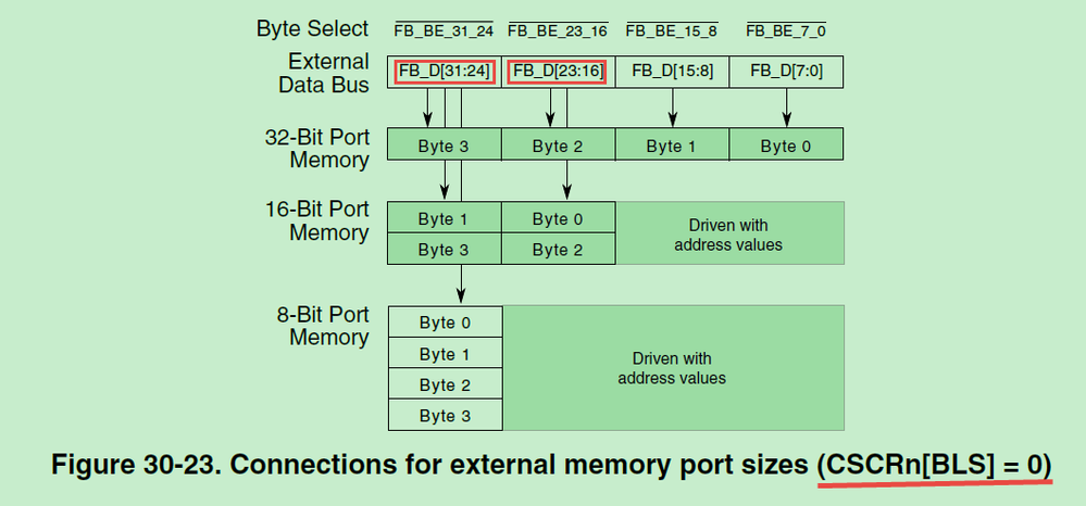
From attached code, the 16-bit data port seems using FB_AD[31:24] pins as data port, which should belongs to below connection:
Then the CSCRn[BLS] bit should be 0.
As this connection, the FB_AD[31:24] should be 16-bit data port's high byte; and FB_AD[23:16] should be the low byte of 16-bit data port.
If it is possible, if customer could post the Flexbus related schematics for the double check.
Wish it helps.
Have a great day,
Ma Hui
-----------------------------------------------------------------------------------------------------------------------
Note: If this post answers your question, please click the Correct Answer button. Thank you!
-----------------------------------------------------------------------------------------------------------------------
