- NXP Forums
- Product Forums
- General Purpose MicrocontrollersGeneral Purpose Microcontrollers
- i.MX Forumsi.MX Forums
- QorIQ Processing PlatformsQorIQ Processing Platforms
- Identification and SecurityIdentification and Security
- Power ManagementPower Management
- MCX Microcontrollers
- S32G
- S32K
- S32V
- MPC5xxx
- Other NXP Products
- Wireless Connectivity
- S12 / MagniV Microcontrollers
- Powertrain and Electrification Analog Drivers
- Sensors
- Vybrid Processors
- Digital Signal Controllers
- 8-bit Microcontrollers
- ColdFire/68K Microcontrollers and Processors
- PowerQUICC Processors
- OSBDM and TBDML
-
- Solution Forums
- Software Forums
- MCUXpresso Software and ToolsMCUXpresso Software and Tools
- CodeWarriorCodeWarrior
- MQX Software SolutionsMQX Software Solutions
- Model-Based Design Toolbox (MBDT)Model-Based Design Toolbox (MBDT)
- FreeMASTER
- eIQ Machine Learning Software
- Embedded Software and Tools Clinic
- S32 SDK
- S32 Design Studio
- Vigiles
- GUI Guider
- Zephyr Project
- Voice Technology
- Application Software Packs
- Secure Provisioning SDK (SPSDK)
- Processor Expert Software
-
- Topics
- Mobile Robotics - Drones and RoversMobile Robotics - Drones and Rovers
- NXP Training ContentNXP Training Content
- University ProgramsUniversity Programs
- Rapid IoT
- NXP Designs
- SafeAssure-Community
- OSS Security & Maintenance
- Using Our Community
-
- Cloud Lab Forums
-
- Home
- :
- General Purpose Microcontrollers
- :
- Kinetis Microcontrollers
- :
- K60 DMA ping-pong issue
K60 DMA ping-pong issue
- Subscribe to RSS Feed
- Mark Topic as New
- Mark Topic as Read
- Float this Topic for Current User
- Bookmark
- Subscribe
- Mute
- Printer Friendly Page
K60 DMA ping-pong issue
- Mark as New
- Bookmark
- Subscribe
- Mute
- Subscribe to RSS Feed
- Permalink
- Report Inappropriate Content
Hello everybody!
I'm working on a project for K60 MCU and encountered a weird issue with the DMA controller.
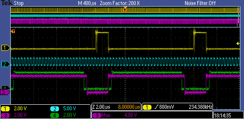
I need to read some data from the ADC. The interface is similar to SAI/I2S, however this ADC is using eight data lines instead of one. That is why I've configured the I2S0 interface to provide SCLK and FSYNC signals and wanted to use DMA for data acquisition. The ADC data outputs are connected to PORT_E[0:7] lines. Whenever we raise FSYNC line the ADC provides us 24 bytes on every raising edge of the SCLK signal (I mean, the time we should read them). Below is an example of saturated output (For clearer visibility FSYNC is raised for 24 SCLK periods).
blue - SCLK, violet - FSYNC (up for 24 periods), green - saturated data (0x7FFFFF), yellow - doesn't matter.
I used SCLK rising edge to trigger the DMA (one byte minor loop, 24 bytes major loop) and FSYNC signal was meant to enable the DMA (which would get disabled after every major loop). Another thing is that I need to do the data postprocessing immediately after I gather the samples and it takes a little bit longer than the time to next FSYNC rise (next data packet). If I used one DMA it would start overwriting the data being currently processed and that's bad. That's why I wanted to use two DMA channels with exactly the same configuration and only one difference: the destination buffer address. They were supposed to run one after another in cycles so I have time to proccess the data.
I tried three different methods to enable the channels on rising FSYNC edge:
- I connected IRQ handling routine to FSYNC (way too slow, especially during read/write operations to external SRAM).
- I used third DMA that copies one predefined byte to DMA_SERQ register. The byte is being changed by both ISR channels (since I was not able to use PORT_A for the third DMA I had to loopback the FSYNC to PORT_D.15)
- It was a variation of the second idea. Third DMA had two bytes in major loop and the source address was a 2-byte array containing DMA_1 and DMA_2 channel numbers. This way I did not have to change anything in the ISR anymore. Below code snippets belong to this version.
Some defines first:
#define I2S0_DMA_SAMPLE_COUNT ( 24 )
#define DMA_ENABLER_CHANNEL   ( 13 )
#define I2S0_DMA_1_CHANNEL    ( 15 )
#define I2S0_DMA_2_CHANNEL    ( 14 )
#define BUF_SIZE              ( 64 )

#define I2S0_DMA_1_VECT_NUM   DMA15_DMA31_IRQn
#define I2S0_DMA_2_VECT_NUM   DMA14_DMA30_IRQn
#define DMA_ENABLER_VECT_NUM  DMA13_DMA29_IRQn
Data structures:
static volatile uint8_t AdcDataBuffer[2][BUF_SIZE] __attribute__((aligned (BUF_SIZE)));
DMA_Type *DmaPtr = DMA0;

uint16_t DmaI2sChan_1   = I2S0_DMA_1_CHANNEL;
uint16_t DmaI2SChan_2   = I2S0_DMA_2_CHANNEL;
uint16_t DmaEnablerChan = DMA_ENABLER_CHANNEL;

static volatile uint8_t DmaEnableValues[2] = {
  I2S0_DMA_1_VECT_NUM,
  I2S0_DMA_2_VECT_NUM,
};
First DMA channel configuration (channel 15):
  DMAMUX0->CHCFG[DmaI2sChan_1] = 0x0;

  /* source address is Port E PDIR register */
  DmaPtr->TCD[DmaI2sChan_1].SADDR     = (uint32_t) &PTE->PDIR;
  /* source does not increment */
  DmaPtr->TCD[DmaI2sChan_1].SOFF      = 0;
  /* source does not increment at the end of the major loop */
  DmaPtr->TCD[DmaI2sChan_1].SLAST     = 0;

  DmaPtr->TCD[DmaI2sChan_1].DADDR     = (uint32_t) &AdcDataBuffer [0];
  DmaPtr->TCD[DmaI2sChan_1].DOFF      = 1;
  DmaPtr->TCD[DmaI2sChan_1].DLAST_SGA = (uint32_t) -I2S0_DMA_SAMPLE_COUNT;

  DmaPtr->TCD[DmaI2sChan_1].CITER_ELINKNO =   I2S0_DMA_SAMPLE_COUNT;
  DmaPtr->TCD[DmaI2sChan_1].BITER_ELINKNO =   I2S0_DMA_SAMPLE_COUNT;
  DmaPtr->TCD[DmaI2sChan_1].NBYTES_MLNO   =   1;
  DmaPtr->TCD[DmaI2sChan_1].ATTR          =   DMA_ATTR_SSIZE (0)
                                            | DMA_ATTR_SMOD  (0)
                                            | DMA_ATTR_DSIZE (0)
                                            | DMA_ATTR_DMOD  (0);

  DMAMUX0->CHCFG[DmaI2sChan_1]  =   DMAMUX_CHCFG_SOURCE (PORTA_DMAMUX_SOURCE)
                                  | DMAMUX_CHCFG_ENBL_MASK;

  DmaPtr->TCD[DmaI2sChan_1].CSR =   DMA_CSR_INTMAJOR_MASK
                                  | DMA_CSR_DREQ_MASK;
  DmaPtr->CERQ = DmaI2sChan_1;
  NVIC_EnableIRQ (I2S0_DMA_1_VECT_NUM);
The only difference for second DMA channel (no. 14) configuration:
  // ...
  DmaPtr->TCD[DmaI2sChan_2].DADDR = (uint32_t) &AdcDataBuffer [1];
  // ...
Here's the enabler DMA configuration:
  DMAMUX0->CHCFG[DmaEnablerChan]            = 0x0;
  DmaPtr->TCD[DmaEnablerChan].SADDR         = (uint32_t) &DmaEnableValues[0];
  DmaPtr->TCD[DmaEnablerChan].SOFF          = 1;
  DmaPtr->TCD[DmaEnablerChan].SLAST         = (uint32_t) -2;
  DmaPtr->TCD[DmaEnablerChan].DADDR         = (uint32_t) 0x4000801b; /* SERQ address */
  DmaPtr->TCD[DmaEnablerChan].DOFF          = 0;
  DmaPtr->TCD[DmaEnablerChan].DLAST_SGA     = 0;
  DmaPtr->TCD[DmaEnablerChan].CITER_ELINKNO = 2;
  DmaPtr->TCD[DmaEnablerChan].BITER_ELINKNO = 2;
  DmaPtr->TCD[DmaEnablerChan].ATTR =   DMA_ATTR_SSIZE(0)
                                     | DMA_ATTR_SMOD (0)
                                     | DMA_ATTR_DSIZE(0)
                                     | DMA_ATTR_DMOD (0);
  DMAMUX0->CHCFG[DmaEnablerChan]   =   DMAMUX_CHCFG_SOURCE (PORTD_DMAMUX_SOURCE)
                                     | DMAMUX_CHCFG_ENBL_MASK;
  DmaPtr->TCD[DmaEnablerChan].CSR  = 0x0;

  DmaPtr->SERQ = DmaEnablerChan;
Port settings for DMA:
  /* SCLK is internally generated on PTA.14 (DMA_1 and DMA_2 on rising edge) */
  PORTA->PCR[14] = PORT_PCR_MUX(6) | PORT_PCR_IRQC(1);

  /* FSYNC is loopbacked to PTD.15 (DMA enabler on rising edge) */
  PORTD->PCR[15] = PORT_PCR_MUX(1) | PORT_PCR_IRQC(1);
IRQ priorities:
  /* lower all priorities */
  for (i = -14; i < 105; i++)
    NVIC_SetPriority (i, 0x7);

  /* raise data processing DMA priorities */
    NVIC_SetPriority (I2S0_DMA_1_VECT_NUM, 0x0);
    NVIC_SetPriority (I2S0_DMA_2_VECT_NUM, 0x0);
DMA priorities:
/* channels 0 to 12 have values 0x80 to 0x8c respectively. */
DMA_DCHPRI0  = 0x80; /* can be preempted, can't preempt */
// ...
DMA_DCHPRI12 = 0x8c;

DMA_DCHPRI13 = 0x4f; /* can preempt, cannot be preempted, highest priority */
DMA_DCHPRI14 = 0x8d;
DMA_DCHPRI15 = 0x8e; /* can be preempted, second to highest priority */
(I think I've tried all possible configurations here without luck).
Below are the DMA finished IRQ handling routines:
void DMA_1_ISR (void)
{
  const uint_16 DmaChannel = I2S0_DMA_1_CHANNEL;


  DmaPtr->CINT = DMA_CINT_CINT (DmaChannel);

  /* data processing */
  process (AdcDataBuffer[0]);
}

void DMA_2_ISR (void)
{
  const uint16_t DmaChannel = I2S0_DMA_2_CHANNEL;

  DmaPtr->CINT = DMA_CINT_CINT (DmaChannel);

  /* data processing */
  process (AdcDataBuffer[1]);
}
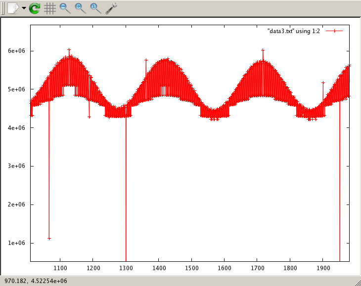
Now here's the issue: Always the channel with higher order number reads corrupted results. If I used (as in example above) channels 14 and 15, data from channel 15 was wrong. If I used 12 and 14, the 14 became corrupted. Nothing changed as I modified the priorities and preemption settings so I assume it has something to do with the DMA channel order.
Here's an example image (every second sample is incorrect but in some regular way):
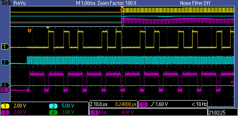
From the image below it looks like the second DMA always kicks off too early. The weird thing is that the data (inspected in the debugger) do look OK actually. I enabled DMA13 HALF and MAJOR interrupts to check if maybe the third DMA was causing the issue but they both were in correct places (right after the FSYNC rising edge).
blue - SCLK, violet - FSYNC (up for 24 periods), yellow - data postprocessing in DMA ISR.
I've already spent too much time on this issue but maybe I'm missing something obvious here? I've already tried many different settings and combinations before giving up this implementation.
For those who are interested in what is my current solution...
I'm using one DMA channel. After it enters the ISR it immediately changes DMA_TCD_DADDR register value to next buffer address and then begins data processing.
The main modifiaction is in the DMA_1 ISR:
static volatile uint_8 AcquisitionBuffer = I2S0_DMA_1_DATA_BUF;

// ...

void DMA_1_ISR (void)
{
  DMA_Type * const DmaPtr       = DMA0;
  const uint_16    DmaChannel   = I2S0_DMA_1_CHANNEL;
  const uint_8     BufToProcess = AcquisitionBuffer;

  AcquisitionBuffer = (AcquisitionBuffer + 1) & 0x1;
  DmaPtr->TCD[DmaChannel].DADDR = (uint32_t) &AdcDataBuffer [AcquisitionBuffer];

  DmaPtr->CINT = DMA_CINT_CINT (DmaChannel);

  /* data processing */
  process (AdcDataBuffer[BufToProcess]);
}
If somebody has an idea what could be incorrect in my setup, please let me know. I'd like to make sure that it's still a software issue and not hardware related.
Thank you,
Matt
- Mark as New
- Bookmark
- Subscribe
- Mute
- Subscribe to RSS Feed
- Permalink
- Report Inappropriate Content
Dear Matt,
I appreciate your patience on this issue and not sure if your problem has been solved!
we have a document AN4590 which is using DMA to emulate ADC scale mode, the case is similar with your application.
the document is available at:
http://cache.freescale.com/files/32bit/doc/app_note/AN4590.pdf
since we dont have your board and schematic, it is not easy for me to find the root reason causing the wrong data read from higher DMA channel.
and dont know exactly the reason causing the early kick off the the second DMA channel.
I hope AN4590 helps, if your problem still there, then, please reply!
- Mark as New
- Bookmark
- Subscribe
- Mute
- Subscribe to RSS Feed
- Permalink
- Report Inappropriate Content
Dear Mr. Yong,
Thank you for the answer. Unfortunately the Flexible Scan mode is not suitable here as I need exactly 24 DMA triggers synchronized with SCLK and they (as a group) must be synchronized with FSYNC signal. I didn’t read the AN4590 document before but came up with similar solution (as I wrote in the forum):
- One DMA channel gathers 24 bytes, gives IRQ when it finishes (where I reconfigure its destination buffer and do the data postprocessing) and automatically disables itself
- Second DMA channel is triggered by FSYNC and the only thing it does, it writes a predefined one-byte command to appropriate register that enables first DMA which will start data acquisition immediately with next SCLK slope. This DMA runs continuously and does not trigger any IRQ-s.
The only thing I was unable to do is to use third DMA channel and run two of them one after another in cycles. I could avoid changing the destination buffer in the IRQ this way but I first thought it would not work after all. It works quite nicely though.
I’m sorry but I didn’t have much time to extract a very simple proof-of-concept example. To me it seems that something may be wrong with the hardware as I spent nearly two weeks and checked all possible settings combinations.
A simple scenario that could help you reproduce the weird behavior (if you’d like to let someone investigate it):
- Use one DMA that runs continuously and enables two DMA channels one by one (I used a two-byte source buffer with appropriate SERQ register values)
- Second DMA gathers 24 bytes in a major loop (one byte minor loop), triggers IRQ and disables itself
- Third DMA does exactly the same but they differ in destination buffer address
- Everything runs at 30 MHz / 256 frequency.
- Provide some arbitrary data from reliable source and check if both DMA transfers give you correct values.
Regards,
Mateusz


