- NXP Forums
- Product Forums
- General Purpose MicrocontrollersGeneral Purpose Microcontrollers
- i.MX Forumsi.MX Forums
- QorIQ Processing PlatformsQorIQ Processing Platforms
- Identification and SecurityIdentification and Security
- Power ManagementPower Management
- MCX Microcontrollers
- S32G
- S32K
- S32V
- MPC5xxx
- Other NXP Products
- Wireless Connectivity
- S12 / MagniV Microcontrollers
- Powertrain and Electrification Analog Drivers
- Sensors
- Vybrid Processors
- Digital Signal Controllers
- 8-bit Microcontrollers
- ColdFire/68K Microcontrollers and Processors
- PowerQUICC Processors
- OSBDM and TBDML
-
- Solution Forums
- Software Forums
- MCUXpresso Software and ToolsMCUXpresso Software and Tools
- CodeWarriorCodeWarrior
- MQX Software SolutionsMQX Software Solutions
- Model-Based Design Toolbox (MBDT)Model-Based Design Toolbox (MBDT)
- FreeMASTER
- eIQ Machine Learning Software
- Embedded Software and Tools Clinic
- S32 SDK
- S32 Design Studio
- Vigiles
- GUI Guider
- Zephyr Project
- Voice Technology
- Application Software Packs
- Secure Provisioning SDK (SPSDK)
- Processor Expert Software
-
- Topics
- Mobile Robotics - Drones and RoversMobile Robotics - Drones and Rovers
- NXP Training ContentNXP Training Content
- University ProgramsUniversity Programs
- Rapid IoT
- NXP Designs
- SafeAssure-Community
- OSS Security & Maintenance
- Using Our Community
-
-
- Home
- :
- General Purpose Microcontrollers
- :
- Kinetis Microcontrollers
- :
- why the voltage of RESET pin of KE02Z MCU is unstable?
why the voltage of RESET pin of KE02Z MCU is unstable?
- Subscribe to RSS Feed
- Mark Topic as New
- Mark Topic as Read
- Float this Topic for Current User
- Bookmark
- Subscribe
- Mute
- Printer Friendly Page
- Mark as New
- Bookmark
- Subscribe
- Mute
- Subscribe to RSS Feed
- Permalink
- Report Inappropriate Content
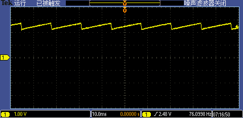
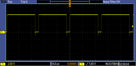
I have a minimum system with the Freescale KE02Z64 MCU,and there are just three parts--power supply circuit, reset circuit and crystal oscillator in this system. then i try to load code to the MCU with the JTAG interface using PE multilink universal. but I failed. the problem is that the signal of restet pin is as follow,
P.S. the power is +5V.
p.p.s. the MCU is newly-welded,no codes in it. it's the first time to use the MCU.
p.p.p.s.the reset circuit and clock circuit are as follow.
how should i deal with this problem? i am needling your help?
Solved! Go to Solution.
- Mark as New
- Bookmark
- Subscribe
- Mute
- Subscribe to RSS Feed
- Permalink
- Report Inappropriate Content
Hello MA QINDONG:
Your last comment:
only the USB LED the on PE multilink universal illumines ,the TGTPWR LED on PE did not illumine
That is not good. Both LEDs have to be ON. Check that the TVCC pin of the JTAG/SWD connector is connected to VCC. And in general check that the MCU is properly powered (VCC and GND pins connected).
Regards!,
Jorge Gonzalez
-----------------------------------------------------------------------------------------------------------------------
Note: If this post answers your question, please click the Correct Answer button. Thank you!
-----------------------------------------------------------------------------------------------------------------------
- Mark as New
- Bookmark
- Subscribe
- Mute
- Subscribe to RSS Feed
- Permalink
- Report Inappropriate Content
Hi,
On a blank device, all of the flash memory sits at the erased state 0xFF (except address 0x0000_040C FSEC which is 0xFE).
You fit the device to your board, and apply power, then core goes to 0x0000_0000 to fetch the initial stack pointer and 0x0000_0004 to fetch the reset vector. Both of these read 0xFFFF-FFFF and so these are illegal addresses. This causes the chip resets, and starts all over again.
The symptom is that the reset line oscillates as the chip runs (reset high) then resets (reset low). It's not unexpected.
You will find useful the information on this post and the answers on a thread:
PE multilink JTAG/BDM Kinetis programming issue | Freescale Community
How To Sucessfully Program a Custom made Kinetis Microcontroller Board.
:smileyinfo: Please consider posting your questions into the right community place for better visibility, for example Kinetis Microcontrollers.
I hope this information can help you.
Regards,
Adrian
-----------------------------------------------------------------------------------------------------------------------
Note: If this post answers your question, please click the Correct Answer button. It would be nice!
-----------------------------------------------------------------------------------------------------------------------
- Mark as New
- Bookmark
- Subscribe
- Mute
- Subscribe to RSS Feed
- Permalink
- Report Inappropriate Content
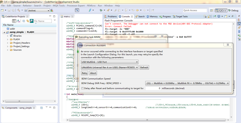
thank you for your response. i have followed the references you give. but there still exists a trouble, my CW10.6 can not connect to the P&E device(this error exists all the time ). the error i get was:
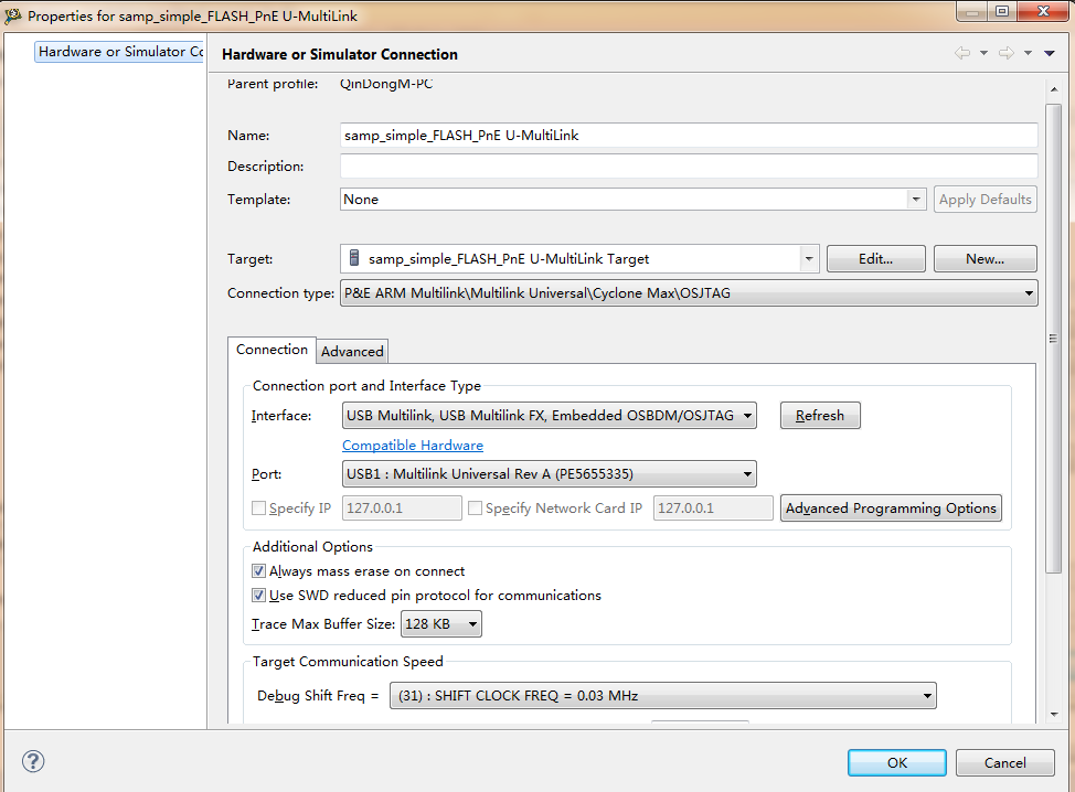
the debug configuration i set was shown as follows:
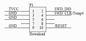
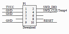
and the JTAG connector i adopted was:
p.s. there is no pull-up resister in SWD_DIO pin. Actually, i have tried to add one, but it didn't work.
p.p.s. the pull-up resister in RESET pin has been replaced by a 10kΩ one, and the capacitor has been taken off.
p.p.p.s. the codes can been loaded to another board(freesacle's FRDM-KE02Z) with the same P&E multilink universal.
- Mark as New
- Bookmark
- Subscribe
- Mute
- Subscribe to RSS Feed
- Permalink
- Report Inappropriate Content
- Mark as New
- Bookmark
- Subscribe
- Mute
- Subscribe to RSS Feed
- Permalink
- Report Inappropriate Content
Yong Li,thank you for your advice. i have referred to the material you send me. and i have checked my custom board carefully. but i have not found any solutions. here i list my board's routing.
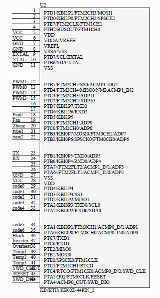
1, all the VDDs including Pin 6 of the MCU(U2) have connected to VCC(+5V) . all VSSes including Pin 7 &Pin 8 have connected to GND. all of these pins have tested.
2, SWD_CLK and SWD_DIO connect directly to P1. p.s. the Temp4 which share with SWD_CLK has been taken off. both SWD_CLK and SWD_DIO connect no external pull-up/down resistors. actually, i have tried to add a 10kΩ pull-up resistor to SWD_DIO and a 10kΩ pull-down resistor to SWD_CLK, but i didn't work.
3, the reset pin of U2 connects to a 10kΩ pull-up resistor without capacitor.
4, other pins except for mentioned above were suspended.
in this condition, i got the signal of MCU's reset pin was:
is it reasonable? it seems to be different from https://community.freescale.com/docs/DOC-99609 .
and if i connect my board to CW10.6 by P&E multilink universal , the CW report disconnecting error,
of course, only the USB LED the on PE multilink universal illumines ,the TGTPWR LED on PE did not illumine.
how can i do to handle with my trouble?
- Mark as New
- Bookmark
- Subscribe
- Mute
- Subscribe to RSS Feed
- Permalink
- Report Inappropriate Content
Hello MA QINDONG:
Your last comment:
only the USB LED the on PE multilink universal illumines ,the TGTPWR LED on PE did not illumine
That is not good. Both LEDs have to be ON. Check that the TVCC pin of the JTAG/SWD connector is connected to VCC. And in general check that the MCU is properly powered (VCC and GND pins connected).
Regards!,
Jorge Gonzalez
-----------------------------------------------------------------------------------------------------------------------
Note: If this post answers your question, please click the Correct Answer button. Thank you!
-----------------------------------------------------------------------------------------------------------------------
- Mark as New
- Bookmark
- Subscribe
- Mute
- Subscribe to RSS Feed
- Permalink
- Report Inappropriate Content
DONE!!! thank you for your advice! i checked my board carefully, yes, it's empty solder. after amending this mistake, i succeeded to erase the virgin MCU.
p.s. i succeeded with no pull-up in SWD_DIO and no pull-down in SWD_CLK. if i added these two resistors, i failed. i didn't know the reason. anyhow, i can program the MCU now.
at last, i am very grateful to all those helped me!
best regards.
- Mark as New
- Bookmark
- Subscribe
- Mute
- Subscribe to RSS Feed
- Permalink
- Report Inappropriate Content
Hi,
Good to know that now it is working!
Best regards,
Adrian
