
- NXP Forums
- Product Forums
- General Purpose MicrocontrollersGeneral Purpose Microcontrollers
- i.MX Forumsi.MX Forums
- QorIQ Processing PlatformsQorIQ Processing Platforms
- Identification and SecurityIdentification and Security
- Power ManagementPower Management
- MCX Microcontrollers
- S32G
- S32K
- S32V
- MPC5xxx
- Other NXP Products
- Wireless Connectivity
- S12 / MagniV Microcontrollers
- Powertrain and Electrification Analog Drivers
- Sensors
- Vybrid Processors
- Digital Signal Controllers
- 8-bit Microcontrollers
- ColdFire/68K Microcontrollers and Processors
- PowerQUICC Processors
- OSBDM and TBDML
-
- Solution Forums
- Software Forums
- MCUXpresso Software and ToolsMCUXpresso Software and Tools
- CodeWarriorCodeWarrior
- MQX Software SolutionsMQX Software Solutions
- Model-Based Design Toolbox (MBDT)Model-Based Design Toolbox (MBDT)
- FreeMASTER
- eIQ Machine Learning Software
- Embedded Software and Tools Clinic
- S32 SDK
- S32 Design Studio
- Vigiles
- GUI Guider
- Zephyr Project
- Voice Technology
- Application Software Packs
- Secure Provisioning SDK (SPSDK)
- Processor Expert Software
-
- Topics
- Mobile Robotics - Drones and RoversMobile Robotics - Drones and Rovers
- NXP Training ContentNXP Training Content
- University ProgramsUniversity Programs
- Rapid IoT
- NXP Designs
- SafeAssure-Community
- OSS Security & Maintenance
- Using Our Community
-
-
- Home
- :
- Product Forums
- :
- Vybrid Processors
- :
- VIU3 to I2C SCL interference?
VIU3 to I2C SCL interference?
- Subscribe to RSS Feed
- Mark Topic as New
- Mark Topic as Read
- Float this Topic for Current User
- Bookmark
- Subscribe
- Mute
- Printer Friendly Page
- Mark as New
- Bookmark
- Subscribe
- Mute
- Subscribe to RSS Feed
- Permalink
- Report Inappropriate Content
Hi
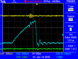
I have some weird I2C2 SCL clock issue. Please see attached oscillogram.
Digital chn 0 and analogue chn 1 is I2C2 SCL signal
Digital chn 1 - I2C2 SDA
Digital chn 2 - one of VIU3 pixel data inputs
Digital chn 3 - VIU3 HSYNC input
Digital chn 5 - VIU3 PIXEL_CLK input
It seems SCL high pulse can be abandoned by VIU3 pixel data. No matter what's pixel clock, is it 10MHz or 40MHz, SCL still may get broken. I have 3rd party CMOS camera module attached to TVR-VF65GS10 card. This camera module for some reason passes SCL through integrating RC circuit with R=22 Ohm, C=680pF. That's why SCL rising edges are quite round. Issue persists even if I reduce SCL frequency to <10kHz (which I think should make rising time relatively short to be relevant). Luckily I have workaround for this problem, making SCL pin fully driven and not open drain solves the issue.
What's worse, once such short SCL pulse is generated, I2C module seems entering some weird state. For example sometimees I see bus busy in status register, though I2C and SCL both are idling high and MSSL=0.
Am I wrong in thinking that once I2C wins arbitration, nothing on SCL or SDA should be able to shorten SCL-high pulses. Isn't it? SCL-low can be stretched by slave device, but SCL-high shouldn't be affected, right?
If it matters here's connection list:
// cmos_pixclk pci_primary_a8 ptb15
// cmos_hsync pci_primary_b40 ptb6 ? J23 remove jumper from pin 4, SCI2_TX; or keep unused
// cmos_vsync pci_primary_b39 ptb7 J24 remove jumper from pin 4, SCI2_RX; or keep unused
// cmos_d0 pci_primary_a19 ptc3
// cmos_d1 pci_primary_a20 ptc4
// cmos_d2 pci_primary_b13 ptc5
// cmos_d3 pci_primary_b19 ptc6
// cmos_d4 pci_primary_b20 ptc7
// cmos_d5 pci_primary_b46 ptb19
// cmos_d6 pci_primary_b44 ptb20
// cmos_d7 pci_primary_b45 ptb21
// cmos_d9 pci_primary_a22 pta16 don't enable trace d0 14
// cmos_d9 pci_primary_a39 ptb1 yellow LED 19
// cmos_d10 pci_primary_a38 ptb2 yel/grn LED
// cmos_d11 pci_primary_a37 ptb3 or/red LED 21
I2C2 SCL PTA22
I2C2 SDA PTA23
Any ideas?
Thanks
Solved! Go to Solution.
- Mark as New
- Bookmark
- Subscribe
- Mute
- Subscribe to RSS Feed
- Permalink
- Report Inappropriate Content
Hi Edward,
Thanks for the feedback. Looks like the camera is built to try to avoid cross coupling.
We have found through simulation that a glitch (or spike) can actually trigger the observed behavior. We are now investigating further.
If you ever see an opportunity to capture the rising edge of SCL for the error case, that would still be helpful as it will give us some data to match against.
Best regards,
Richard
- Mark as New
- Bookmark
- Subscribe
- Mute
- Subscribe to RSS Feed
- Permalink
- Report Inappropriate Content
(corrected-2)
Hello Edward,
Still not clear if relevant or not, but on the TWR-VF65GS10 card schematic, the PTA22 line (used as I2C2 SCL by you) is shared, it specifically comes to the Elevator connector J17A, so question - are you using the card itself or the Tower kit as a whole, and if the latter, are you sure there is no influence on the PTA22 line from the rest of the kit?
This assumption is based on your information - "Luckily I have workaround for this problem, making SCL pin fully driven and not open drain solves the issue". And "luckily" your SCL outpur is stronger than that "parasite's" one applying the opposite logic level (Low in your case). It is not that safe, to have 2 outputs fighting each other, BTW - some times one of them gets "killed".
Regards, Naoum Gitnik.
- Mark as New
- Bookmark
- Subscribe
- Mute
- Subscribe to RSS Feed
- Permalink
- Report Inappropriate Content
Hello Naoum and thanks for your interest
I'm using TWR-VF65GS10 card alone. J17B PCI-E connector is not connected, J17A PCI-E connector is connected to camera adapter PCB. I found pins to use on Vybrid card that are not shared or which are connected to unconnected connectors pins etc so no two signal sources are driving the same wire.
"Luckily" - I mean my product protype will work any way, is there problem in Vybrid chip or not, I have solution for this = disable SCL open drain. Series current limiting resistor will solve ouput current limit specifications.
Regards
Edward
- Mark as New
- Bookmark
- Subscribe
- Mute
- Subscribe to RSS Feed
- Permalink
- Report Inappropriate Content
Hello Edward,
Unfortunately, I do not remember all details of the I2C protocol but, if I am not wrong, clock always comes from the Master, right?
And who is a Master in your scheme?
And where do you change the output type on the clock signal - Vybrid or the camera? And in general - if behavior changes after this change, most likely it means some other "body" is also driving this open-drain/collector line with a shared pull-up resistor (so-called "wired OR" scheme).
BTW, "The bus is a multi-master bus which means any number of master nodes can be present. Additionally, master and slave roles may be changed between messages (after a STOP is sent)." [I²C - Wikipedia, the free encyclopedia] - possible root cause...?
Another detail I found - "SCL ... is generated by the master device and controls when data is sent and when it is read... can be forced low so that no clock can occur. This is done by a device that has become too busy to accept more data." [http://ww1.microchip.com/downloads/en/devicedoc/i2c.pdf]
Regards, Naoum Gitnik.
- Mark as New
- Bookmark
- Subscribe
- Mute
- Subscribe to RSS Feed
- Permalink
- Report Inappropriate Content
Hello Naoum,
I2C is multimaster protocol and I mentioned I2C bus master arbitration because I believe that 1) SCL-high can't be shortened by slave or other masters, unless two masters are trying to win arbitration while generating I2C-Start at the same time, 2) even if slave fails for some reason and pulls SCL low in the middle of SCL-high, I2C master should keep SCL relesed (high) for expected programmed SCL high time, but oscillogram looks like some internal SCL high counter prematurely signals "done". In addition to distorted SCL clock I2C module enters some weird nonresponsive state, which I can't characterize in all details. Sometimes it is bus busy with MSSL==0 and SDL==SDA==high, which survives toggling MDIS bit to 1 and than to 0. Sometimes I2C status regsiter signals transfer in progress. In all such cases I can't I2C-start and send again, I2C module is stuck until reset.
- Mark as New
- Bookmark
- Subscribe
- Mute
- Subscribe to RSS Feed
- Permalink
- Report Inappropriate Content
Hi Edward,
I had a look at the scope image that you attached earlier.
I don't think there is any clock stretching in that signal. We seem to be missing part of the clock pulse. Or prematurely done condition as you call it.
I'm wondering if maybe software incidentally re-programs the SCL clock timing, causing it to prematurely start a new clock cycle. This is inspired by the fact that it seems to correlate withH-Sync, independent of frequencies. Maybe Software wants to adjust timing to accommodate the VIU and in the process resets the SCK timing reference.
There's quite a bit of guesswork in this reply, but since there is very little chance that H-Sync can affect I2C in some hardware way, it's more likely software related.
Best regards,
Richard
- Mark as New
- Bookmark
- Subscribe
- Mute
- Subscribe to RSS Feed
- Permalink
- Report Inappropriate Content
Hi Richard,
I believe software isn't reprogramming SCL clock timing. If it was true, then I would see the same or similar behaviour with SCL made not open drain. Enabling SCL upper side driver fixes the issue. Also I'm not using H-sync interrupt or waiting for and using H-sync status flag.
- Mark as New
- Bookmark
- Subscribe
- Mute
- Subscribe to RSS Feed
- Permalink
- Report Inappropriate Content
Hi Edward,
That's a good point. I did actually read that but I did not realize that it made things work correctly.
Now, that leads me to the following theory.
The I2C controller monitors SCL signal to detect any clock stretches by the slave. The detection of a rising edge on SCL starts the next cycle (bit).
Now, that detector may also trigger on glitches causing the controller to prematurely start the next cycle, which would result in a signal like the one you captured, The glitch can be introduced by capacitive coupling with some other signal.
If you are using wires for the I2C signals in the setup with the tower board, you may try using shielded wiring for I2C, or prevent glitches being picked-up in another way.
Also make sure both boards have a solid common ground point to avoid any ground noise.
I hope this will help to make it work correctly.
Best regards,
Richard
- Mark as New
- Bookmark
- Subscribe
- Mute
- Subscribe to RSS Feed
- Permalink
- Report Inappropriate Content
Hi Richard,
I have sensor adapter PCB that plugs directly to primary side PCI-E connector on Vybrid card. Sensor is 3.3V powered from Vybrid card, there's no Vcc or Vdd difference, possibility of current injection effects is eliminated.
I2C clock stretching is what slaves are using for handshaking. When slave is busy, it pulls SCL low. Master may release SCL while it is pulled low by slave, but has to wait for SCL==1 before starting counting SCL-high time. This is how SCL clock stretching is supposed to work. So what you see on my oscillogram can't be explained by SCL clock stretching.
Regards
- Mark as New
- Bookmark
- Subscribe
- Mute
- Subscribe to RSS Feed
- Permalink
- Report Inappropriate Content
Hi Edward,
Yes, clock stretching is supposed to lengthen the low-period of the SCL. it's also only supposed to be used for standard mode operation. However, I was not saying that this was some kind of clock stretching.
What I meant to say was that I think glitches on the SCL signal may cause the the transmitter state machine in the I2C controller to prematurely start the next bit. I do not know the internals of this I2C controller so I do not know this for sure, but I have seen such things happen in the past on other devices.
The glitches that I refer to will be like spikes of a few 100 mV sitting on the rising edge of the clock, around the threshold level of the input buffer (at roughly 1.5V). They may only visible on a high-frequency scope.
If glitches are the problem, it may help to turn-on Hysteresis on the I/O pad.
Best regards,
Richard
- Mark as New
- Bookmark
- Subscribe
- Mute
- Subscribe to RSS Feed
- Permalink
- Report Inappropriate Content
Hi Richard,
Of course I tried enabling and disabling pad hysteresis. It didn't make any change. Regarding glitch, of course I could try chasing it with high-freq scope. But it doesn't make a lot of sense to spend my time on it. In the worst case I'll use more robust software emulated I2C...
- Mark as New
- Bookmark
- Subscribe
- Mute
- Subscribe to RSS Feed
- Permalink
- Report Inappropriate Content
Hi Edward,
That should be OK.
I think we can conclude from your observations that the clock pulse can be shortened by external events.
Since the issue doesn't occur when the SCL pin is configured as output (no open drain) means that it must be caused by an external event as the only difference on-chip is the lower output impedance of the pin.
I'm fairly confident that you will not see this issue on the final PCB when traces will probably much shorter. On the current tower board, the SCL trace is uite long as can be seen below.

If you have not done so already, you could try to replace the 4.7K pull-up with a lower value (1.5K or even 470 Ohm), but I don't know if it will make much difference.
Thanks for reporting the issue. Let us know if there is anything else we can do to help.
Best regards,
Richard
- Mark as New
- Bookmark
- Subscribe
- Mute
- Subscribe to RSS Feed
- Permalink
- Report Inappropriate Content
Hi Richard,
I'm not so optimistic regarding final product PCB, which will operate in quite harsh environment. In current dev. setup SCL and SDA look very clean to me. Parhaps lower SCL R*C will make ir solved, but I still thing something is wrong in Vybrid chip, I2C must be more robust.
Regards
- Mark as New
- Bookmark
- Subscribe
- Mute
- Subscribe to RSS Feed
- Permalink
- Report Inappropriate Content
Hi Edward,
I have already requested design to lo check the I2C module to understand how exactly the pulse gets shortened. Based on that we will be able to judge what the next steps need to be..
In that respect, what is the frequency of the IP bus clock in your system?
It also occurred to me that you may be able to fix the problem by enabling the digital filter on the PTA22 input. I have never used this myself, but it should work if I understand things correctly.
The filter configuration is in the PORT module and PTA22 is on PORT0[12]. You can set the filter to use the bus clock. The filter length determines for how many continuous filter clock cycles the input signal must be in the same state before the new state will propagate into Vybrid. I recon a filter delay of ~100 ns should be sufficient.
Hope this works for you,
Best regards,
Richard
- Mark as New
- Bookmark
- Subscribe
- Mute
- Subscribe to RSS Feed
- Permalink
- Report Inappropriate Content
Hi Richard,
Thanks for digital filter idea. I forgot about presence of this feature. Unfortunately it doesn't help. I enabled digital filter for I2C2 SDA and SCL on PTA22 and PTA23 as follows, verified DS-5 debugger registers view shows right values. No change for better, unfortunately:
PORT0->DFER |= (1<<13)|(1<<12);
PORT0->DFWR = 0x1F;
I'm not sure what is IP bus clock, Vybrid RM is full of different names for the same thing. I guess it is IPG_CLK_DIV output clock as shown in fig. 9-1 Clock Generation and Distribution.
I'm using two clocking configurations, same problem with both:
1)
500MHz core,
500/3=166.6MHz platform bus clock
166.6/2=83.3MHz IPG_CLK_DIV output
2)
266MHz core,
266/2=133MHz platform bus clock
133/2 = 65.5MHz IP_CLK_DIV output
Regards
P.S. I thought topic starter is one who marks replies helpful or solution correct. Someone is doing this job for me :-)
- Mark as New
- Bookmark
- Subscribe
- Mute
- Subscribe to RSS Feed
- Permalink
- Report Inappropriate Content
Hi Edward,
Thanks for the feedback. I have passed on the frequencies to design. I hope to get a reply in the next few days,
For the digital filter, did you set the filter length (DFWR) before enabling the filter? The reference manual states that DFWR must only be changed when all filters are disabled. I do not know what the reason for that requirement is but it is easy to try if it was not already in that order.
For the marker, I never mark my own replies. Somtimes the community admins mark a reply as helpful.
- Mark as New
- Bookmark
- Subscribe
- Mute
- Subscribe to RSS Feed
- Permalink
- Report Inappropriate Content
Hi Richard,
Thanks, good point. Just tried swapping those two lines, DFWR is inialized first. Still no change.
Regards
- Mark as New
- Bookmark
- Subscribe
- Mute
- Subscribe to RSS Feed
- Permalink
- Report Inappropriate Content
Hi Edward,
The design team is looking at the I2C module to understand where the issue may be.
Now the design engineer asks if you can try running the i2C at a much slower system clock, like 5 to 20 MHz and check if the problem still exists.
He also asked about lowering the pull-up resistance. Have you tried that already?
Is it possible for you to try the above?
I also had them check the input path and found that the digital filter on the PAD only works for GPIO, so that will help for the I2C input. (I have already marked the reference manual with this update).
Best regards,
Richard
- Mark as New
- Bookmark
- Subscribe
- Mute
- Subscribe to RSS Feed
- Permalink
- Report Inappropriate Content
Hi Richard,
Thanks for investigating I2C module. I'm not sure if I made clear before that I2C SCL clock distortion happens only when there's some activity on VIU3 data input wires. I don't know how to determine which wire causes the problem, but I2C clock distortion always happens during CMOS camera row data transfer. It never happens while camera data wires are idle. I tried reducing camera sensivity so that all wires idle low - no problem. I tried skiping IOMUX initialization for VIU3 pads, leaving them in reset default state - problems still appears. Looks like it is noise produced by camera wires. But how does it upset I2C and doesn't generate problems with A5 code, USB, QSPI or CAN?
I tried lowering IPG frequency gradually down to 20.8MHz. Problems persists at every BUS_CLK and IPG_CLK divider setting I tried. I can't try lower freqs at the moment, some part of software, which I use to trigger I2C transfers can't go slower.
Regarding lowering pull up resistors. Isn't it enough to reduce SCL clock frequency instead? I doubt it.
Thanks for information about digital filter. I think it could be useful not only for GPIO.
Best regards,
Edward
- Mark as New
- Bookmark
- Subscribe
- Mute
- Subscribe to RSS Feed
- Permalink
- Report Inappropriate Content
Hi Edward,
Thanks for testing. At this point we're trying to find an explanation for what we see happen.
My guess is that the video data creates a glitch on the SCL line. It is probably not a single data line, but a group of data lines all switching from low to high at the same time. For example video signal goes from black to white or so.
When the edges on the video data signals are very fast (dv/dt = high) this may cross-couple onto other signals.
Slow rising edges are particularly sensitive to this because the signal level will transition slowly through the threshold region. During that transition it may pick up this noise and this noise may look like a clock edge to the input. I.e. the clock input sees 2 clock edges instead of 1. It will typically look like this:

Since you still see it occur at 20 MHz IPG clock, you may actually be able to see it on a 40 or 100 MHz scope as well.
Best regards,
Richard
- Mark as New
- Bookmark
- Subscribe
- Mute
- Subscribe to RSS Feed
- Permalink
- Report Inappropriate Content
I'm seeing pretty much the same thing, talking to a CRTOUCH chip using a Kinetis K70. My FAE tells me that the K70 uses essentially the same I2C IP as the Vybrid, so maybe my problems have the same root cause?
My system is using a custom board with a K70 processor. On the board, the I2C signals travel about 3", then enter a flat flex circuit that is about 10" long, before finally getting to the CRTOUCH chip. Along that flex cable runs 24 lines of LCD video data, as well as the pixel clock and line/frame sync pulses. So there are a lot of high frequency signals in that cable that could be cross-talking to the I2C lines. There are no other I2C devices on that bus: the K70 is the master, and the CRTOUCH chip is the only slave.
I get these glitches at random intervals, but on the average they are a little more frequent than once a second. I attempt to read from the bus every 25 ms, so I get a glitch that causes a bad read about every 35 reads, or a bit less than once every 2800 clock cycles.
While I don't have as nice a scope as Edward, I was able to get a couple screen captures that I hope might be useful. In each screen shot, the yellow trace is a GPIO output that software strobes when the I2C read call returns an error. Cyan is the SCL line. Green is SDA.
F0136TEK.BMP shows a truncated clock cycle. There is the normal low period, a short high-going glitch, followed by another normal low period. The data line changes just after the glitch, which makes me think that the I2C peripheral just skipped the high portion of the clock, and continued on immediately with the next clock cycle.
F0139TEK.BMP is a closeup of a truncated clock pulse. Looking at the scope earlier, I first thought that the glitches on the yellow trace were just scope artifacts caused by poor probe grounding and long fly-wire lengths leading to the probes. But when zoomed in, it's clear that the yellow glitch happens before the falling edge of the clock pulse, so it's likely not a scope artifact caused by the clock switching. At the same time, there is a similar glitch in the blue SCL line, and about 100 ns later the pulse is truncated. The glitch looks to be on the order of a couple hundred mV. This sure sounds a lot like the failure scenario being described.
F0139CH2.CSV is a data export of the cyan SCL trace from F0139TEK.BMP, which gives the measured voltage for each sample. Maybe this extra detail might help the analysis effort?
I have not yet tried Edward's signal drive work-around, or the other filtering tips provided in this thread. That will come next.
I hope this information helps.
-- Adam