- NXP Forums
- Product Forums
- General Purpose MicrocontrollersGeneral Purpose Microcontrollers
- i.MX Forumsi.MX Forums
- QorIQ Processing PlatformsQorIQ Processing Platforms
- Identification and SecurityIdentification and Security
- Power ManagementPower Management
- MCX Microcontrollers
- S32G
- S32K
- S32V
- MPC5xxx
- Other NXP Products
- Wireless Connectivity
- S12 / MagniV Microcontrollers
- Powertrain and Electrification Analog Drivers
- Sensors
- Vybrid Processors
- Digital Signal Controllers
- 8-bit Microcontrollers
- ColdFire/68K Microcontrollers and Processors
- PowerQUICC Processors
- OSBDM and TBDML
-
- Solution Forums
- Software Forums
- MCUXpresso Software and ToolsMCUXpresso Software and Tools
- CodeWarriorCodeWarrior
- MQX Software SolutionsMQX Software Solutions
- Model-Based Design Toolbox (MBDT)Model-Based Design Toolbox (MBDT)
- FreeMASTER
- eIQ Machine Learning Software
- Embedded Software and Tools Clinic
- S32 SDK
- S32 Design Studio
- Vigiles
- GUI Guider
- Zephyr Project
- Voice Technology
- Application Software Packs
- Secure Provisioning SDK (SPSDK)
- Processor Expert Software
-
- Topics
- Mobile Robotics - Drones and RoversMobile Robotics - Drones and Rovers
- NXP Training ContentNXP Training Content
- University ProgramsUniversity Programs
- Rapid IoT
- NXP Designs
- SafeAssure-Community
- OSS Security & Maintenance
- Using Our Community
-
-
- Home
- :
- i.MX Forums
- :
- i.MX Processors
- :
- RL(Read Latency) bit of EIM in i.MX6DL.
RL(Read Latency) bit of EIM in i.MX6DL.
- Subscribe to RSS Feed
- Mark Topic as New
- Mark Topic as Read
- Float this Topic for Current User
- Bookmark
- Subscribe
- Mute
- Printer Friendly Page
RL(Read Latency) bit of EIM in i.MX6DL.
- Mark as New
- Bookmark
- Subscribe
- Mute
- Subscribe to RSS Feed
- Permalink
- Report Inappropriate Content
Dear Sir or Madam,
Refer to 22.9.4 Chip Select n Read Configuration Register 2 (EIM_CSnRCR2) in MCIMX6SDLRM(Rev.1).
[Q1]
Refer to RL bit.
Are "cycle" and EIM_clock the meaning?
[Q2]
RL bit can define "Feedback clock loop delay".
What is Feedback clock loop delay?
And, how should I set RL bit?
Keita
- Mark as New
- Bookmark
- Subscribe
- Mute
- Subscribe to RSS Feed
- Permalink
- Report Inappropriate Content
1.
The RL field holds the feedback clock loop delay in aclk cycle units.
ACLK_EIM_SLOW_CLK_ROOT is source clock for the EIM, mentioned often as
"ACLK", "AXI clock" and "EMI clock".
2.
From section 22.2.1 (Other Important Block I/O Signals Internal to the SoC) of the i.MX6SDL RM :
Feedback clock is used to sample read data during high transfer speeds. The signal provides feedback
from the I/O pad of the BCLK output pin and tends to align more closely with data from the external memory
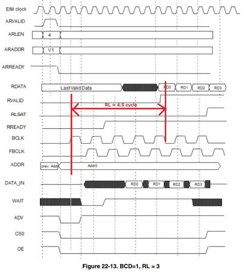
device. Please look at Figure 22-13 (BCD=1, RL = 3).
- Mark as New
- Bookmark
- Subscribe
- Mute
- Subscribe to RSS Feed
- Permalink
- Report Inappropriate Content
Dear Yuri,
Thank you for your reply.
2.
> Please look at Figure 22-13 (BCD=1, RL = 3)
I looked Figure 22-13.
I didn't understand the relation of FBCLK & RDATA.
How should I decide the RL value?
Keita
- Mark as New
- Bookmark
- Subscribe
- Mute
- Subscribe to RSS Feed
- Permalink
- Report Inappropriate Content
Actually waveform figures in the Reference Manual are provided mainly as demonstration material and do not reflect all timing aspects.
RL field in some sense defines data hold time. It should match BCD field.
- Mark as New
- Bookmark
- Subscribe
- Mute
- Subscribe to RSS Feed
- Permalink
- Report Inappropriate Content
Hi Yuri,
I checked a SRAM datasheet about read latency, and I feel RL indicates from latching address to output read data as attached image.
When BCD=1 & RL=3, read latency is 4.5 cycle as the above image, right?
If it is right, the Figure 22-12 does NOT indicate correct read latency, it seems 5 cycles even though it should be 1 cycle since BCD=0 & RL=0.
Would you give us a comment about it?
Best Regards,
Satoshi Shimoda
- Mark as New
- Bookmark
- Subscribe
- Mute
- Subscribe to RSS Feed
- Permalink
- Report Inappropriate Content
As has been mentioned, the pictures in the RM do not refelect exactly timing relationships.
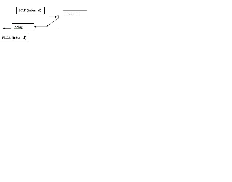
RL parameters control loop delay between the I/O pad of the BCLK and the FBCLK (internal
signal), which is used to sample read data.
~Yuri.
- Mark as New
- Bookmark
- Subscribe
- Mute
- Subscribe to RSS Feed
- Permalink
- Report Inappropriate Content
Hello Yuri,
Let me confirm folloiwng three points regarding FB_BCLK.
- RL and FB_BCLK are only used when Continous BCLK mode, and they are also used in DLL internally for better syncronization.
- They don't affect on Data Read timing. so it's ok just looking at rising edge of the BCLKs to know when the Data is sampled.
- When BCD is used, Continous BCLK cannot be used then FB_BCLK is no use.
Are these understandings correct?
Best regards,
Nori Shinozaki
- Mark as New
- Bookmark
- Subscribe
- Mute
- Subscribe to RSS Feed
- Permalink
- Report Inappropriate Content
Please look at my comments below.
1)
> RL and FB_BCLK are only used when Continous BCLK mode, and they are also
> used in DLL internally for better syncronization.
RL and FB_BCLK are used for any synchronous accesses.
2)
> They don't affect on Data Read timing. so it's ok just looking at rising edge of
> the BCLKs to know when the Data is sampled.
RL affects the Data Read timing, since it provides additional tuning for data latch timing.
3)
> When BCD is used, Continous BCLK cannot be used then FB_BCLK is no use.
This is not so. RL and FB_BCLK are used for any synchronous accesses.
~Yuri.

