
- NXP Forums
- Product Forums
- General Purpose MicrocontrollersGeneral Purpose Microcontrollers
- i.MX Forumsi.MX Forums
- QorIQ Processing PlatformsQorIQ Processing Platforms
- Identification and SecurityIdentification and Security
- Power ManagementPower Management
- MCX Microcontrollers
- S32G
- S32K
- S32V
- MPC5xxx
- Other NXP Products
- Wireless Connectivity
- S12 / MagniV Microcontrollers
- Powertrain and Electrification Analog Drivers
- Sensors
- Vybrid Processors
- Digital Signal Controllers
- 8-bit Microcontrollers
- ColdFire/68K Microcontrollers and Processors
- PowerQUICC Processors
- OSBDM and TBDML
-
- Solution Forums
- Software Forums
- MCUXpresso Software and ToolsMCUXpresso Software and Tools
- CodeWarriorCodeWarrior
- MQX Software SolutionsMQX Software Solutions
- Model-Based Design Toolbox (MBDT)Model-Based Design Toolbox (MBDT)
- FreeMASTER
- eIQ Machine Learning Software
- Embedded Software and Tools Clinic
- S32 SDK
- S32 Design Studio
- Vigiles
- GUI Guider
- Zephyr Project
- Voice Technology
- Application Software Packs
- Secure Provisioning SDK (SPSDK)
- Processor Expert Software
-
- Topics
- Mobile Robotics - Drones and RoversMobile Robotics - Drones and Rovers
- NXP Training ContentNXP Training Content
- University ProgramsUniversity Programs
- Rapid IoT
- NXP Designs
- SafeAssure-Community
- OSS Security & Maintenance
- Using Our Community
-
-
- Home
- :
- Product Forums
- :
- Vybrid Processors
- :
- Workaround for unreliable boot from SD?
Workaround for unreliable boot from SD?
- Subscribe to RSS Feed
- Mark Topic as New
- Mark Topic as Read
- Float this Topic for Current User
- Bookmark
- Subscribe
- Mute
- Printer Friendly Page
- Mark as New
- Bookmark
- Subscribe
- Mute
- Subscribe to RSS Feed
- Permalink
- Report Inappropriate Content
I've been testing a TWR-VF65GS10 Rev. G board built with the full tower (main board + TWR-SER2 module + TWR-LCD-RGB module) and noticed that the board boot ROM does not reliably boot from the SD card on each reset. I'm using the 4GB SanDisk MicroSD card that came with the board. I have both the micro-USB port on the main board (J3) and the mini-USB connector on the primary elevator board attached to my development machine to power the system. Once every 15-20 cold power cycles (by toggling the power switch on the primary elevator board), the board fails to run U-Boot from the SD card. The same failure also occasionally occurs when pressing the reset button on the main board or when using a hardware debugger (attached to the 20-pin JTAG connector) to issue a warm reset. I haven't noticed any difference in the frequency of the failure between cold and warm resets. This behavior occurs regardless of whether the JTAG hardware debugger is attached to the board, but when the JTAG debugger is attached, I can see that the PC is at an address within the boot ROM (e.g. PC=0x000030c0 or 0x00006ba6) after the failure occurs. We've had two engineers both independently discover this issue on different boards so it doesn't appear to be a problem with one particular board. Is there a workaround for this issue that will allow us to reliably boot from the SD card?
Solved! Go to Solution.
- Mark as New
- Bookmark
- Subscribe
- Mute
- Subscribe to RSS Feed
- Permalink
- Report Inappropriate Content
Hi,
- No, Reset does not help here.
- We are having plans to improve the POR block in the next board revision, and using a voltage supervisor is one of the options.
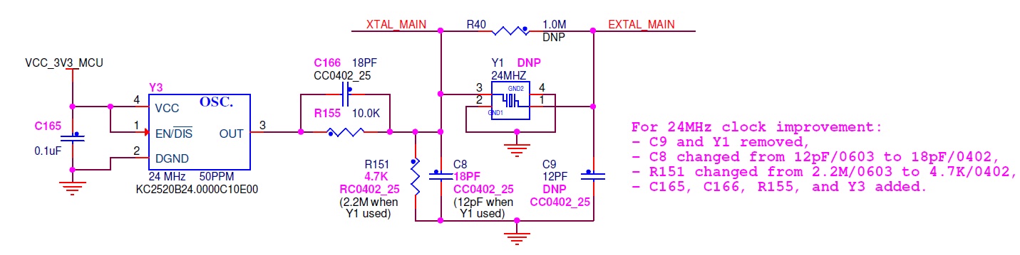
- This approach is copied from the oscilloscope probe design (see attached).
- If all the parasitic capacitance sources are taken into account (~14pF), the capacitance ratio becomes close to the ideal 1:2; the actual ratio deviates a little from it to prevent having an additional component type on the BOM, but the simulation results are still good enough.
Regards, Naoum Gitnik.
- Mark as New
- Bookmark
- Subscribe
- Mute
- Subscribe to RSS Feed
- Permalink
- Report Inappropriate Content
Dear Ian,
- Try lowering the C8 and C9 value to 3.9...6.8pF from 12pF (near the Y1 crystal).
- If your application does not need clocks to be very accurate (within a few tens of ppm), most likely you may simply try removing C8 (perhaps C9 as well).
Please, let me know which one of the solutions, 1 or 2, you tried and how well it worked for you.
Regards, Naoum Gitnik.
- Mark as New
- Bookmark
- Subscribe
- Mute
- Subscribe to RSS Feed
- Permalink
- Report Inappropriate Content
I too need the processor to boot reliably. I'm a bit confused by the above cap change suggestions since they are so different from our earlier exchange. Did you discover that the I/O pin capacitance (inside chip) is much larger than the DS currently states (9pF) so that we don't need much/any external capacitance for the crystal to oscillate? And/or, is the Tower board contributing more stray pcb capacitance than earlier estimated? I see the logical progression here and it could make perfect sense, it's just that it's quite abnormal to not have load caps on a crystal. And, unfortunately, I do require good accuracy, <5 ppm at 25C.
Maybe a Plan B option is to revisit publishing a "known to work" oscillator circuit to avoid all of the above issues? Thanks, Chris
- Mark as New
- Bookmark
- Subscribe
- Mute
- Subscribe to RSS Feed
- Permalink
- Report Inappropriate Content
Dear Ian and Chris,
It is more or less the same e5881 erratum from the previous chip revision"Errata":
System Boot:
BootROM might use UART as boot device instead of the requested boot device.
Description:
The device may boot into UART boot mode instead of the configured boot mode if the external crystal oscillator (FXOSC) startup time is greater than 1.4ms.
Workaround:
1. Higher load crystal capacitance will lead to longer startup times, decrease the crystal load capacitance to decrease startup time.
2. Use an external clock with a startup time of 1.4ms or less to provide a 1.1V peak-to-peak signal input to the XTAL pin.
We considered it fixed in the current chip revision; unfortunately, it appeared to be fixed only partially, so we are in process of adding a similar erratum into the current "Errata".
We are also working on fixing the problem properly in the next chip revision (December-January timeframe).
If high accuracy required, an external clock source can be used. It should be taken into account, though, that the voltage swing used by Vybrid is up to 1.1V, so the best solution would be using a 3.3V rated clock oscillator with a voltage "2:1"divider on the output (built of Rs and Cs due to high frequency - see example attached, untested but simulated).
Regards, Naoum Gitnik.
- Mark as New
- Bookmark
- Subscribe
- Mute
- Subscribe to RSS Feed
- Permalink
- Report Inappropriate Content
Naoum,
I wonder where could I find document that includes e5881 errata? I found only erratas for 1N02G maskset VYBRID_1N02G. It doesn't include e5881.
- Mark as New
- Bookmark
- Subscribe
- Mute
- Subscribe to RSS Feed
- Permalink
- Report Inappropriate Content
Hello Edward,
This new erratum is already in process of being added into the existing Errata document; unfortunately, I cannot tell its publication date, but expect it quite soon.
BTW, it is important to know that the required clock "readiness" time got a bit shorter - 1.2 ms, not 1.4.
Regards, Naoum Gitnik.
- Mark as New
- Bookmark
- Subscribe
- Mute
- Subscribe to RSS Feed
- Permalink
- Report Inappropriate Content
Good explanation. To clarify, I can't fix it with Reset, right? It's a race condition AFTER Reset is released (Reset=1 turns on EXTAL to start the crystal oscillations). I just want to get a good picture of what's really happening since it helps me get comfortable on the oscillator side (no race condition there since oscillator will be easily up at the end of my Reset deassertion)
Follow-up to above, any chance changing from RC reset circuit to voltage supervisor chip would help? I'm a fan of supervisors which you might consider as a default on the Tower (as opposed to RC) then let customers take the more aggressive (risky) move of deleting it for cost reasons if they can convince themselves that it won't cause issues (brownout hang). Or maybe this was all thought out and it would just help to hear the reasoning behind the RC choice and why there isn't a brownout hang risk. Relying on CPU-internal brownout circuits makes me a bit nervous since it might suffer from the same type of intermediate voltage hang (brownout) as the CPU, but maybe it was built in a different manner (from CPU), effectively an external watchdog that just happens to be on the die with the CPU.
I really like the simple oscillator R-divider circuit. I compute worst case 1.07V max for 1% resistors.
Could you explain the use of the two 18 pF caps on the R-ladder? Thanks, Chris
- Mark as New
- Bookmark
- Subscribe
- Mute
- Subscribe to RSS Feed
- Permalink
- Report Inappropriate Content
Hi,
- No, Reset does not help here.
- We are having plans to improve the POR block in the next board revision, and using a voltage supervisor is one of the options.
- This approach is copied from the oscilloscope probe design (see attached).
- If all the parasitic capacitance sources are taken into account (~14pF), the capacitance ratio becomes close to the ideal 1:2; the actual ratio deviates a little from it to prevent having an additional component type on the BOM, but the simulation results are still good enough.
Regards, Naoum Gitnik.