
- NXP Forums
- Product Forums
- General Purpose MicrocontrollersGeneral Purpose Microcontrollers
- i.MX Forumsi.MX Forums
- QorIQ Processing PlatformsQorIQ Processing Platforms
- Identification and SecurityIdentification and Security
- Power ManagementPower Management
- MCX Microcontrollers
- S32G
- S32K
- S32V
- MPC5xxx
- Other NXP Products
- Wireless Connectivity
- S12 / MagniV Microcontrollers
- Powertrain and Electrification Analog Drivers
- Sensors
- Vybrid Processors
- Digital Signal Controllers
- 8-bit Microcontrollers
- ColdFire/68K Microcontrollers and Processors
- PowerQUICC Processors
- OSBDM and TBDML
-
- Solution Forums
- Software Forums
- MCUXpresso Software and ToolsMCUXpresso Software and Tools
- CodeWarriorCodeWarrior
- MQX Software SolutionsMQX Software Solutions
- Model-Based Design Toolbox (MBDT)Model-Based Design Toolbox (MBDT)
- FreeMASTER
- eIQ Machine Learning Software
- Embedded Software and Tools Clinic
- S32 SDK
- S32 Design Studio
- Vigiles
- GUI Guider
- Zephyr Project
- Voice Technology
- Application Software Packs
- Secure Provisioning SDK (SPSDK)
- Processor Expert Software
-
- Topics
- Mobile Robotics - Drones and RoversMobile Robotics - Drones and Rovers
- NXP Training ContentNXP Training Content
- University ProgramsUniversity Programs
- Rapid IoT
- NXP Designs
- SafeAssure-Community
- OSS Security & Maintenance
- Using Our Community
-
-
- Home
- :
- Product Forums
- :
- S12 / MagniV Microcontrollers
- :
- MM912G634DV1AE Programming
MM912G634DV1AE Programming
- Subscribe to RSS Feed
- Mark Topic as New
- Mark Topic as Read
- Float this Topic for Current User
- Bookmark
- Subscribe
- Mute
- Printer Friendly Page
- Mark as New
- Bookmark
- Subscribe
- Mute
- Subscribe to RSS Feed
- Permalink
- Report Inappropriate Content
Hi
I have problem for programming with MM912G634DV1AE , my programmer is MULTILINK UNIVERSAL I have error with subject about can not write in 0xFFF8!
what is your suggestion ?
Solved! Go to Solution.
- Mark as New
- Bookmark
- Subscribe
- Mute
- Subscribe to RSS Feed
- Permalink
- Report Inappropriate Content
I tested low side driver at MM912F634 device and you are right Low side driver didn’t work as I expected.
There are several errata for low side driver at analog die:
http://www.freescale.com/files/analog/doc/errata/MM912F634ER.pdf
Unfortunately I am not expert for analog die (I focus mainly on S12 MCUs) therefore I cannot simply explain root cause of this issue.
I discover that there is some issue with bg1p25sleep reference and this reference has to be trimmed.
Please add this code prior low side driver initialization:
/* Analog Die Trim */
MMCCTL1 = 0x01; // Enable IFR Read
B_CTR2 = 0x1E; //trim bg1p25sleep reference
I tested SLPBGTR2…0 values and any value between 0b000 and 0b110 works fine on my board (B_CTR2 value between 0x1B and 0x1E).
I hope it helps you.
Edit: I tested also MM912H634 (MM912G634) device and Low Side Switch works fine without any trimming.
Just:
B_LSCEN = 0x05; // Enable LS Control
B_LSCR = 0x03; // Activate LS1 + LS2
Message was edited by: Radek Sestak
- Mark as New
- Bookmark
- Subscribe
- Mute
- Subscribe to RSS Feed
- Permalink
- Report Inappropriate Content
Dear Radek
For programming I connect TCLK to +12 V
1- do you have sample code for watchdog and trim and LIN ?
2-for interrupter need to rest each ISR register after use it ?How can I Reset ISR interrupt?
this is my code
interrupt 6 void D2D(void)
{
// ISR = 0 , 0 , HOT , LSOT , HSOT, LINOT, SCI ,RX ,TX ,ERR ,TOV, CH3 ,CH2 ,CH1 , CH0 , VSI
volatile int16u ivr,isr;
volatile int8u B_WSR_reg = 0;
ivr = B_IVR;
isr = B_ISR;
if (ivr == 0)
{
B_WSR_reg = B_WSR; // remove interrupt flag
}
if ( isr & 0x10) //TC3 interrupt
{
B_TC3 = B_TCNT + 40000; //set TC3 as output compare when TCRE = 0
B_PTB_PTB2 = !B_PTB_PTB2; //toggle PA7
boolTickTimer = ON;
B_TFLG1 = 0x08; //clear C3F flag when TFFCA=0
}
if (isr & 0x0080)// TX interrupt
{
if ( B_SCIS1_TDRE && B_SCIC2_TIE)// B_SCIS1_TC &&
{
if ( LINStateManage() == FALSE )
{
structLinFrameBuffer.enuState = LIN_STATE_IDLE ;
}
B_SCIS1_TDRE = 1;
}
}
if (isr == 0x0100)// RX interrupt
{
if (B_SCIS2_LBKDIF && B_SCIBDH_LBKDIE) // A break signal was received
{
structLinFrameBuffer.enuState =LIN_STATE_BREAK_FIELD;
structLinFrameBuffer.int8uSynchPointer=0;
B_SCIS2_LBKDIF = 1;
}
if( (B_SCIS1_RDRF || B_SCIS1_OR) && B_SCIC2_RIE) // interrupt of Receive
{
B_SCIS1_RDRF = 1;
B_SCIS1_OR =1;
structLinFrameBuffer.enuState = LIN_STATE_SYNC_FIELD;
structLinFrameBuffer.int8uSynch[SYNCHFIELD] = B_SCID;
if ( LINStateManage() == FALSE )
{
structLinFrameBuffer.enuState = LIN_STATE_IDLE ;
}
BackLightWindowSwitch =1;
}
}
}
- Mark as New
- Bookmark
- Subscribe
- Mute
- Subscribe to RSS Feed
- Permalink
- Report Inappropriate Content
Dear Radek
My problem has open , I can not use LOW side out put? LOW side pin out put contact to relay and i did follow with debuger in MM912H register are intial
B_LSCEN = 0x05;
B_LSCR = 0x03;
after intial i saw with debuger that is is equal with
B_LSCEN = 0x05;
B_LSCR = 0; !!!!!!!!!
1- why it can not write 0x03 in B_LSCR ?
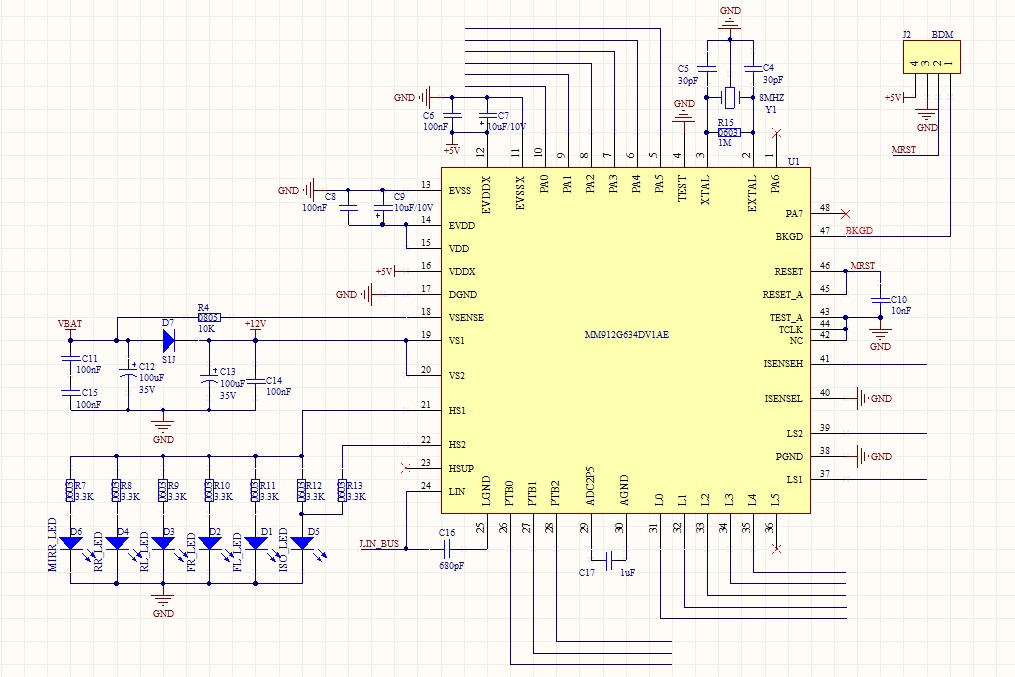
2- need to special note to hardware ? please check our schematic in enclosed.
thanks,
- Mark as New
- Bookmark
- Subscribe
- Mute
- Subscribe to RSS Feed
- Permalink
- Report Inappropriate Content
I checked you scheme and I would like to notice that assembled oscillator circuit looks fine for MM912F634 device.
However CPMU block in MM912G(H)634 support only Loop Control Pierce Oscillator connection (or internal RC oscillator) and you have not populate R15 in case assembled MM912G634 or MM912H634.
- Mark as New
- Bookmark
- Subscribe
- Mute
- Subscribe to RSS Feed
- Permalink
- Report Inappropriate Content
I tested low side driver at MM912F634 device and you are right Low side driver didn’t work as I expected.
There are several errata for low side driver at analog die:
http://www.freescale.com/files/analog/doc/errata/MM912F634ER.pdf
Unfortunately I am not expert for analog die (I focus mainly on S12 MCUs) therefore I cannot simply explain root cause of this issue.
I discover that there is some issue with bg1p25sleep reference and this reference has to be trimmed.
Please add this code prior low side driver initialization:
/* Analog Die Trim */
MMCCTL1 = 0x01; // Enable IFR Read
B_CTR2 = 0x1E; //trim bg1p25sleep reference
I tested SLPBGTR2…0 values and any value between 0b000 and 0b110 works fine on my board (B_CTR2 value between 0x1B and 0x1E).
I hope it helps you.
Edit: I tested also MM912H634 (MM912G634) device and Low Side Switch works fine without any trimming.
Just:
B_LSCEN = 0x05; // Enable LS Control
B_LSCR = 0x03; // Activate LS1 + LS2
Message was edited by: Radek Sestak
- Mark as New
- Bookmark
- Subscribe
- Mute
- Subscribe to RSS Feed
- Permalink
- Report Inappropriate Content
thank you so much Radek.
my problem is solved but I have MM912H and MM912F for both of them i need to trimming but you say it is only for MM912F I should be check with MM912G and tell you about result,
thanks again,
- Mark as New
- Bookmark
- Subscribe
- Mute
- Subscribe to RSS Feed
- Permalink
- Report Inappropriate Content
1- for mass production RESET_A pin has to be connected to RESET pin or not?if yes for programming has not problem?
2- I have only MM912F in my hand and I want write software in mm912F after development switch to MM912G is it possible ?
3- Now I have new problem I could not toggle pins of PORTA and PORTB in output ?why? has a special note?run D2DI has a note?
looking forward to your comment .
thanks
- Mark as New
- Bookmark
- Subscribe
- Mute
- Subscribe to RSS Feed
- Permalink
- Report Inappropriate Content
- During programming in mass production and debugging – at least 8V has to be connected to TCLK pin. If is it not possible (error on PCB), you can temporary disconnect RESET_A and RESET pins during programming (after that connect back).
- Yes, it is possible. You can write software for MM912F634 and after that you can migrate (with some software changes) this code to MM912G634.
- There isn’t anything special. Port A is located at MCU therefore you need only set DDR register to output mode. Port B is located at analog die therefore you need initialize D2D interface and set DDR bits to output mode. In attachment you can find simple example code.
- Mark as New
- Bookmark
- Subscribe
- Mute
- Subscribe to RSS Feed
- Permalink
- Report Inappropriate Content
thank you so much for your help,
Now I disconnected RESET_A to RESET before programming after that contact again to RESET but micro can not run again!!! Micro burst is reset ?why?
1- do you think are there any problem in my schematic ?
2- why my micro burst is reset?
- Mark as New
- Bookmark
- Subscribe
- Mute
- Subscribe to RSS Feed
- Permalink
- Report Inappropriate Content
Your program contains a function for periodically resetting of window watchdog?
If yes, please check if you feed watchdog in proper time interval (second half of timeout period).
If not, please add function for feed watchdog or connect at least 8V to TCLK pin.
- Mark as New
- Bookmark
- Subscribe
- Mute
- Subscribe to RSS Feed
- Permalink
- Report Inappropriate Content
I contacted at least 8V to TCLK pin and solved my problem,
now i have two question :
1- how can i use interrupt timer?
2- what is interrupt vector for Timer ?
3-do you have source code for init timer ?
4- I can not use Low side driver i'd write
| B_LSCEN | = 0x05; | |
| B_LSCR | = 0x03; |
and for disable B_LSCR = 0;
why I can not use it?it has a special note?Alse I can use High side driver without any problem.
- Mark as New
- Bookmark
- Subscribe
- Mute
- Subscribe to RSS Feed
- Permalink
- Report Inappropriate Content
About 1..3)
Timer is located on analog die therefore you should use D2D interrupt for handling Timer interrupt.
D2D Interface interrupt vector is Vector base + 0x00F2 (interrupt 6).
Yes, in atachment you can find simple example code for MM912H634.
About 4)
Strange, it works correctly on my side. What you have connected to LS pins?
- Mark as New
- Bookmark
- Subscribe
- Mute
- Subscribe to RSS Feed
- Permalink
- Report Inappropriate Content
- Mark as New
- Bookmark
- Subscribe
- Mute
- Subscribe to RSS Feed
- Permalink
- Report Inappropriate Content
could you help with sample code ?I could not toggle pins of PORTA and PORTB in output ?why? hse a special note?D2DI has a note?
thanks,
- Mark as New
- Bookmark
- Subscribe
- Mute
- Subscribe to RSS Feed
- Permalink
- Report Inappropriate Content
- Mark as New
- Bookmark
- Subscribe
- Mute
- Subscribe to RSS Feed
- Permalink
- Report Inappropriate Content
The problem is: If voltage at TCLK pins is bellow 7V, window watchdog at analog die will be active and Initial Non-window Watchdog Timeout is just 150ms (110…190ms). So, you have to program MCU in shorter time than 110ms (after reset) or you have to make some hardware changes for programming.
Recommendation:
- Disassemble R15. MM912G634 supports only Loop Controlled Pierce Oscillator Connection (see Figure 83. OSCLCP Block Diagram).
- Disable window watchdog or disconnect reset signal.
- Disable window watchdog – disconnect TCLK pin from GND and connect TCLK pin to GND by pull-down resistor. During programming just connect at least 8V to TCLK pin.
- Disconnect reset signal – window watchdog is located on analog die, if you disconnect RESET_A and RESET pins, analog die will not cause MCU reset. RESET signal must stay connected to BDM interface.
Note: There is third option, connect just +5V to VDDX for powering MCU, however we strictly not recommend this solution.
- Mark as New
- Bookmark
- Subscribe
- Mute
- Subscribe to RSS Feed
- Permalink
- Report Inappropriate Content
thanks a lot for your information,
yesterday I can program of course my problem was RESET_A .
Now RESET_A pin always should be disconnect to GND or contact to GND with separate capacitor ?
- Mark as New
- Bookmark
- Subscribe
- Mute
- Subscribe to RSS Feed
- Permalink
- Report Inappropriate Content
RESET_A pin has to be connected to RESET pin.
I would like to recommend disconnect RESET_A and RESET pins only for programming (watchdog on analog die will not interrupt MCU) - as workaround in production.
For debugging purpose is better connecting at least 8V to TCLK pin. This will disable window watchdog and you can fully use both dies.
If you connect at least 8V to TCLK pin, RESET_A pin could be connected to RESET pin all the time.
- Mark as New
- Bookmark
- Subscribe
- Mute
- Subscribe to RSS Feed
- Permalink
- Report Inappropriate Content
Mr.Radek Sestak
I test with your software and I have this problem again,
Error is : " Error while writing to FFFE..101FE"
what is your suggestion ?
- Mark as New
- Bookmark
- Subscribe
- Mute
- Subscribe to RSS Feed
- Permalink
- Report Inappropriate Content
Strange, everything works correctly on my side.
Please check if you have at least 8V at TCK pin (44). This disable internal watchdog – it is necessary during loading software and debugging.
Are you sure that you have MM912G634 and not MM912F634?
Could you please try connecting to MCU and check Part ID (addresses 0x001A and 0x001B)? There should be 0x38C0 in case of MM912G634 or MM912H634. In case of MM912F634 it should be 0x3800 or 0x3801.
Please check if you already install CodeWarrior for HCS12(X) v5.1 MM912H634 Service Pack:
http://www.freescale.com/webapp/sps/site/overview.jsp?code=CW_UPDATES_HCS12_51
Example codes which I posted above contain small error. There is wrong unsecure command file (old version - it fits to MM912F634). However this should not have any connection to your issue. In attachment you can find correct cmd file for MM912G634 and MM912H634 devices.
If you use KIT912H634 evaluation board, please disconnect JP14 and JP15 jumpers (this disconnect TBDML interface).
If you use KIT912H634 evaluation board, please connect JP6 and set JP7 jumper to position 1-2 (this disable internal watchdog.
- Mark as New
- Bookmark
- Subscribe
- Mute
- Subscribe to RSS Feed
- Permalink
- Report Inappropriate Content
thank you so much for your following,
I have MM912H634 and MM912F634 together ,i could not program into both of them.
about part ID i checked and for 912H is 0xID3 for 912G is 0x1E1 and 912F is 0x1D4.of course this numbers write in our code warier .
some question :
1- can I write software with MM912G and program on the MM912F or H
2- this problem is for software or hardware
3- your attachment was incorrect please sent me again or sent me simple sample because only i want make sure that this problem is for soft ware or hardware
thanks a lot