- NXP Forums
- Product Forums
- General Purpose MicrocontrollersGeneral Purpose Microcontrollers
- i.MX Forumsi.MX Forums
- QorIQ Processing PlatformsQorIQ Processing Platforms
- Identification and SecurityIdentification and Security
- Power ManagementPower Management
- MCX Microcontrollers
- S32G
- S32K
- S32V
- MPC5xxx
- Other NXP Products
- Wireless Connectivity
- S12 / MagniV Microcontrollers
- Powertrain and Electrification Analog Drivers
- Sensors
- Vybrid Processors
- Digital Signal Controllers
- 8-bit Microcontrollers
- ColdFire/68K Microcontrollers and Processors
- PowerQUICC Processors
- OSBDM and TBDML
-
- Solution Forums
- Software Forums
- MCUXpresso Software and ToolsMCUXpresso Software and Tools
- CodeWarriorCodeWarrior
- MQX Software SolutionsMQX Software Solutions
- Model-Based Design Toolbox (MBDT)Model-Based Design Toolbox (MBDT)
- FreeMASTER
- eIQ Machine Learning Software
- Embedded Software and Tools Clinic
- S32 SDK
- S32 Design Studio
- Vigiles
- GUI Guider
- Zephyr Project
- Voice Technology
- Application Software Packs
- Secure Provisioning SDK (SPSDK)
- Processor Expert Software
-
- Topics
- Mobile Robotics - Drones and RoversMobile Robotics - Drones and Rovers
- NXP Training ContentNXP Training Content
- University ProgramsUniversity Programs
- Rapid IoT
- NXP Designs
- SafeAssure-Community
- OSS Security & Maintenance
- Using Our Community
-
-
- Home
- :
- i.MX Forums
- :
- i.MX RT
- :
- Re: When using SEMC, about the maximum delay of each signals
When using SEMC, about the maximum delay of each signals
- Subscribe to RSS Feed
- Mark Topic as New
- Mark Topic as Read
- Float this Topic for Current User
- Bookmark
- Subscribe
- Mute
- Printer Friendly Page
- Mark as New
- Bookmark
- Subscribe
- Mute
- Subscribe to RSS Feed
- Permalink
- Report Inappropriate Content
Dear All,
We connect the RT1175 to a FPGA using SEMC. The interface configuration uses SRAM in ASYNC Mode.
In the design analysis process for FPGAs, we need to set the relative relationships between these signals. It must be the maximum delay in the actual worst case, in addition to the logical number of clock cycles.
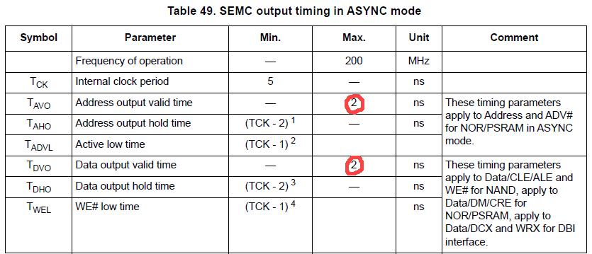
However, the RT1170 data sheet does not list the maximum delay other than Addr and Data.
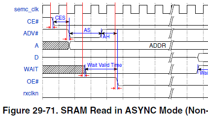
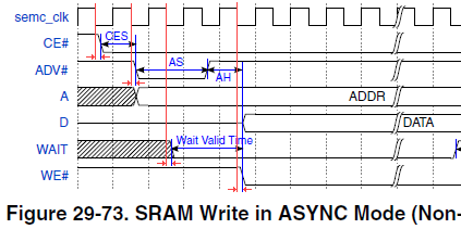
What is the maximum delay of the signals I added in red to the figures in the reference manual?
Should we use 2ns like Addrs and Data, or should we have a larger delay value?
Please tell me reasonable values.
Best Regards,
George
Solved! Go to Solution.
- Mark as New
- Bookmark
- Subscribe
- Mute
- Subscribe to RSS Feed
- Permalink
- Report Inappropriate Content
Hi George,
I received confirmation from IP owner that this won't happen. We have synthesis constraints of these pins and have STA checked for these paths.
Have a great day,
Felipe
-------------------------------------------------------------------------------
Note:
- If this post answers your question, please click the "Mark Correct" button. Thank you!
- We are following threads for 7 weeks after the last post, later replies are ignored. Please open a new thread and refer to the closed one, if you have a related question at a later point in time.
------------------------------------------------------------------------------
- Mark as New
- Bookmark
- Subscribe
- Mute
- Subscribe to RSS Feed
- Permalink
- Report Inappropriate Content
Hi George,
I am going to check internally to see if we have this information available.
Best regards,
Felipe
- Mark as New
- Bookmark
- Subscribe
- Mute
- Subscribe to RSS Feed
- Permalink
- Report Inappropriate Content
- Mark as New
- Bookmark
- Subscribe
- Mute
- Subscribe to RSS Feed
- Permalink
- Report Inappropriate Content
Hi George,
I finally have received an answer about this. Please check it below.
For your question that the time marked in red, the max value is not fixed.
The semc_clk is an internal clock, CE#, ADV#, OE# and WE# are driven at the falling edge of semc_clk, but the time from semc_clk falling edge to CE# falling edge is not a critical timing for accessing.
The access timing is care about the timing between ADDR and ADV#, or DATA and WE#. We don’t need to comment the timing from semc_clk falling edge to CE# or ADV#. Actually it is not available to comment it, because this timing is related with temperature, voltage. The max value should be more than 2ns in worst case.
WAIT pin edge is not related with semc_clk, it is from external device. User need to make sure WAIT valid time should be no less than 2 semc_clk cycles. This timing is configurable by AS and AH fields.
Best regards,
Felipe
-------------------------------------------------------------------------------
Note:
- If this post answers your question, please click the "Mark Correct" button. Thank you!
- We are following threads for 7 weeks after the last post, later replies are ignored. Please open a new thread and refer to the closed one, if you have a related question at a later point in time.
------------------------------------------------------------------------------
- Mark as New
- Bookmark
- Subscribe
- Mute
- Subscribe to RSS Feed
- Permalink
- Report Inappropriate Content
Hello @FelipeGarcia
Thank you for your reply.
First of all, I seem to have misunderstood the function of the WAIT signal. Now I understand it correctly.
Tell me one thing, because our customers want comments from NXP about it.
The access timing is care about the timing between ADDR and ADV#, or DATA and WE#. We don’t need to comment the timing from semc_clk falling edge to CE# or ADV#. Actually it is not available to comment it, because this timing is related with temperature, voltage. The max value should be more than 2ns in worst case.
Does this mean that we can understand it as follows?
CE#, ADV# and WE# can exceed 2ns under the worst conditions of temperature and voltage, but do not exceed 5ns (semc_clk period minimum spec).
Our customers are worried that the signal transition (front and back) order may be reversed.
* I don't think there is an order reversal because each output signal has the same delay increase.
Thanks,
George
- Mark as New
- Bookmark
- Subscribe
- Mute
- Subscribe to RSS Feed
- Permalink
- Report Inappropriate Content
Hi George,
Please see following feedback from internal team.
From gate-level simulation, It can be seen the delay from the falling edge of semc_clk to pins such as CE#, ADV# delay is more than 2ns. And in the worst case, it might be 4ns or 5ns.
Best regards,
Felipe
- Mark as New
- Bookmark
- Subscribe
- Mute
- Subscribe to RSS Feed
- Permalink
- Report Inappropriate Content
Hello @FelipeGarcia,
Thank you for your polite information.
Please only tell us if there is a situation (by minimum and maximum delay in the worst case) where the relationship between each signal is reversed.
*My customer wants the answer in the end.
BR,
George
- Mark as New
- Bookmark
- Subscribe
- Mute
- Subscribe to RSS Feed
- Permalink
- Report Inappropriate Content
Hi George,
Could you please elaborate or give an example of what you are asking? I think I am not quite getting customer request.
Best regards,
Felipe
- Mark as New
- Bookmark
- Subscribe
- Mute
- Subscribe to RSS Feed
- Permalink
- Report Inappropriate Content
Dear @FelipeGarcia,
Sorry for the late reply.
The conditions that my customers are worried about are:
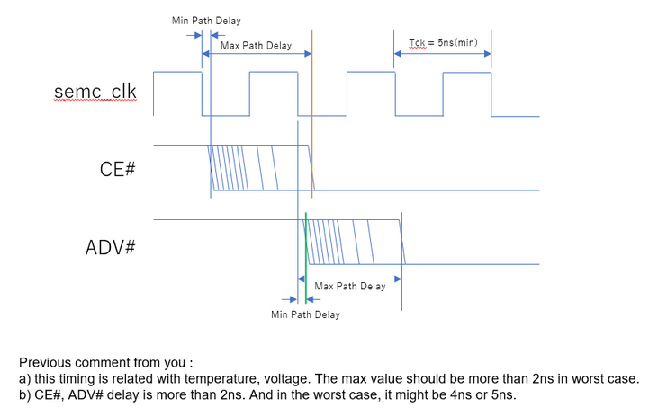
The output signals(CE #, ADV #, A, D, WE #, OE #) associated with semc_clk should have a minimum path and maximum path as output delay from the semc_clk falling edge.
In temperature and voltage are the worst conditions, our customers are worried that the delay difference between the minimum path and maximum path will exceed 5ns(semc_clk min spec).
When using semc_clk with 5ns setting, it will look like the relationship is reversed when viewed from an external chip.
As shown in the figure below, when CE # is MaxPath and ADV # is MinPath, the relationship between the two signals may be reversed.
This example we show is too extreme and may not happen in reality, My customer wants to hear from NXP that it won't happen
We think you can get it by static timing analysis of simulation model.
BR,
George
- Mark as New
- Bookmark
- Subscribe
- Mute
- Subscribe to RSS Feed
- Permalink
- Report Inappropriate Content
Hi George,
I received confirmation from IP owner that this won't happen. We have synthesis constraints of these pins and have STA checked for these paths.
Have a great day,
Felipe
-------------------------------------------------------------------------------
Note:
- If this post answers your question, please click the "Mark Correct" button. Thank you!
- We are following threads for 7 weeks after the last post, later replies are ignored. Please open a new thread and refer to the closed one, if you have a related question at a later point in time.
------------------------------------------------------------------------------
- Mark as New
- Bookmark
- Subscribe
- Mute
- Subscribe to RSS Feed
- Permalink
- Report Inappropriate Content
- Mark as New
- Bookmark
- Subscribe
- Mute
- Subscribe to RSS Feed
- Permalink
- Report Inappropriate Content
Hi @george,
Related team is now in National Holiday so I would expect to have some feedback once it is finished next week.
Best regards,
Felipe


