- NXP Forums
- Product Forums
- General Purpose MicrocontrollersGeneral Purpose Microcontrollers
- i.MX Forumsi.MX Forums
- QorIQ Processing PlatformsQorIQ Processing Platforms
- Identification and SecurityIdentification and Security
- Power ManagementPower Management
- MCX Microcontrollers
- S32G
- S32K
- S32V
- MPC5xxx
- Other NXP Products
- Wireless Connectivity
- S12 / MagniV Microcontrollers
- Powertrain and Electrification Analog Drivers
- Sensors
- Vybrid Processors
- Digital Signal Controllers
- 8-bit Microcontrollers
- ColdFire/68K Microcontrollers and Processors
- PowerQUICC Processors
- OSBDM and TBDML
-
- Solution Forums
- Software Forums
- MCUXpresso Software and ToolsMCUXpresso Software and Tools
- CodeWarriorCodeWarrior
- MQX Software SolutionsMQX Software Solutions
- Model-Based Design Toolbox (MBDT)Model-Based Design Toolbox (MBDT)
- FreeMASTER
- eIQ Machine Learning Software
- Embedded Software and Tools Clinic
- S32 SDK
- S32 Design Studio
- Vigiles
- GUI Guider
- Zephyr Project
- Voice Technology
- Application Software Packs
- Secure Provisioning SDK (SPSDK)
- Processor Expert Software
-
- Topics
- Mobile Robotics - Drones and RoversMobile Robotics - Drones and Rovers
- NXP Training ContentNXP Training Content
- University ProgramsUniversity Programs
- Rapid IoT
- NXP Designs
- SafeAssure-Community
- OSS Security & Maintenance
- Using Our Community
-
-
- Home
- :
- i.MX Forums
- :
- i.MX RT
- :
- Re: What is the function of the DQS line with SDRAM?
What is the function of the DQS line with SDRAM?
- Subscribe to RSS Feed
- Mark Topic as New
- Mark Topic as Read
- Float this Topic for Current User
- Bookmark
- Subscribe
- Mute
- Printer Friendly Page
What is the function of the DQS line with SDRAM?
- Mark as New
- Bookmark
- Subscribe
- Mute
- Subscribe to RSS Feed
- Permalink
- Report Inappropriate Content
What is the purpose and function of the DQS signal in the SEMC SDRAM interface?
- Mark as New
- Bookmark
- Subscribe
- Mute
- Subscribe to RSS Feed
- Permalink
- Report Inappropriate Content
Dear Felipe,
You reported here:
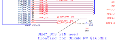
"The recommendation is to leave the pin floating and internal loopback enabled as this is needed for SDRAM read and write operations at 166 MHz, otherwise performance will not be optimal."
This seems to conflict with the IMXRT1064 datasheet where if the loopback is set internal (SEMC_MCR.DQSMD = 0x0) the minimum setup data time is 8.67ns resulting in a maxim speed of around 115MHZ since Hold time is 0ns.
Is it something I am missing?
Moreover if we set the "external loopback" how the SEMC_DQS trace have to be routed in PCB?
Just leave the pad unconnected without any trace?
Kind Regards,
Alessandro
- Mark as New
- Bookmark
- Subscribe
- Mute
- Subscribe to RSS Feed
- Permalink
- Report Inappropriate Content
Hi Gerry,
DQS signal is to compensate the delay of data path and clock. Certain devices use this pin to indicate the dummy cycles needed (before Program/Read data transfer).
Best regards,
Felipe
-------------------------------------------------------------------------------
Note:
- If this post answers your question, please click the "Mark Correct" button. Thank you!
- We are following threads for 7 weeks after the last post, later replies are ignored. Please open a new thread and refer to the closed one, if you have a related question at a later point in time.
------------------------------------------------------------------------------
- Mark as New
- Bookmark
- Subscribe
- Mute
- Subscribe to RSS Feed
- Permalink
- Report Inappropriate Content
Hi Felipe,
Thanks for the response however you don't explain how this is signal is used in the RT1050 with SDRAM. Is it an input to the 1050? If so, how is it used internally and how is it normally connected to external circuitry?
Regards,
Gerry
- Mark as New
- Bookmark
- Subscribe
- Mute
- Subscribe to RSS Feed
- Permalink
- Report Inappropriate Content
Hi Gerry,
SEMC_DQS is input/output when the MCU writes data to the SDRAM, it outputs the DQS in the center of the data it is writing. When reading data, the SDRAM sends the DQS edge aligned with the data.
The recommendation is to leave the pin floating and internal loopback enabled as this is needed for SDRAM read and write operations at 166 MHz, otherwise performance will not be optimal.
Best regards,
Felipe
-------------------------------------------------------------------------------
Note:
- If this post answers your question, please click the "Mark Correct" button. Thank you!
- We are following threads for 7 weeks after the last post, later replies are ignored. Please open a new thread and refer to the closed one, if you have a related question at a later point in time.
------------------------------------------------------------------------------
- Mark as New
- Bookmark
- Subscribe
- Mute
- Subscribe to RSS Feed
- Permalink
- Report Inappropriate Content
Hi Felipe,
Thanks for the information and the recommendation not to use the DQS line. However, I would like to understand it's function in detail. Is there documentation about this functionality with timing diagrams?
Regards,
Gerry
- Mark as New
- Bookmark
- Subscribe
- Mute
- Subscribe to RSS Feed
- Permalink
- Report Inappropriate Content

