- NXP Forums
- Product Forums
- General Purpose MicrocontrollersGeneral Purpose Microcontrollers
- i.MX Forumsi.MX Forums
- QorIQ Processing PlatformsQorIQ Processing Platforms
- Identification and SecurityIdentification and Security
- Power ManagementPower Management
- MCX Microcontrollers
- S32G
- S32K
- S32V
- MPC5xxx
- Other NXP Products
- Wireless Connectivity
- S12 / MagniV Microcontrollers
- Powertrain and Electrification Analog Drivers
- Sensors
- Vybrid Processors
- Digital Signal Controllers
- 8-bit Microcontrollers
- ColdFire/68K Microcontrollers and Processors
- PowerQUICC Processors
- OSBDM and TBDML
-
- Solution Forums
- Software Forums
- MCUXpresso Software and ToolsMCUXpresso Software and Tools
- CodeWarriorCodeWarrior
- MQX Software SolutionsMQX Software Solutions
- Model-Based Design Toolbox (MBDT)Model-Based Design Toolbox (MBDT)
- FreeMASTER
- eIQ Machine Learning Software
- Embedded Software and Tools Clinic
- S32 SDK
- S32 Design Studio
- Vigiles
- GUI Guider
- Zephyr Project
- Voice Technology
- Application Software Packs
- Secure Provisioning SDK (SPSDK)
- Processor Expert Software
-
- Topics
- Mobile Robotics - Drones and RoversMobile Robotics - Drones and Rovers
- NXP Training ContentNXP Training Content
- University ProgramsUniversity Programs
- Rapid IoT
- NXP Designs
- SafeAssure-Community
- OSS Security & Maintenance
- Using Our Community
-
-
- Home
- :
- i.MX Forums
- :
- i.MX RT
- :
- Re: RT1170 ADC Input Voltage
RT1170 ADC Input Voltage
- Subscribe to RSS Feed
- Mark Topic as New
- Mark Topic as Read
- Float this Topic for Current User
- Bookmark
- Subscribe
- Mute
- Printer Friendly Page
- Mark as New
- Bookmark
- Subscribe
- Mute
- Subscribe to RSS Feed
- Permalink
- Report Inappropriate Content
I have some questions related to these forum posts:
https://community.nxp.com/t5/i-MX-RT/MIMXRT1176-LPADC-voltage-reference-scaling/m-p/1386125
https://community.nxp.com/t5/i-MX-RT/RT1170-ADC-reference-voltages/m-p/1475671
1. Does the 30/64 scaling option contribute to measurement errors? I assume there is, since it is an analog function. Or is it so well-controlled that the conversion specs in the datasheet aren't affected?
2. If there is a measurement error, how does it affect differential ADC measurements compared to single-ended?
3. Is VREFH scaled up internally by 64/30? Or is there a voltage reducer of 30/64 on the input to each A/D converter? Or something else? How does CSCALE work its magic?
4. Is an input only damaged when VADIN > NVCC_GPIOmax? For example, if NVCC_GPIO is 3.3V and VREFH is 1.54V, is there any software setting that could result in damage to the chip if VADIN is 3.3V?
5. If NVCC_GPIO is 3.3V, VREFH is 1.8V, and CSCALE is enabled, that would create an internal VREF of 3.84V. I don't even see how that is possible, since NVCC_GPIO (and all other power inputs) would be 3.3V or less. Would that result in any damage?
- Assuming CSCALE reduces VADIN, then the transformed VADIN would be compared to 1.8V?
- Assuming CSCALE increases VREFH internally, then VADIN would be compared to whatever VREFH is internally. Assuming this results in an internal VREF that is equal to NVCC_GPIO, is this a way to achieve conversions that are ratiometric with the 3.3V supply?
6. What is the input impedance of VREFH? The only spec I can find in the datasheet is a maximum supply current of 2 mA. That seems like a pretty low impedance for a reference input.
Thanks!
Regards,
Greg
Solved! Go to Solution.
- Mark as New
- Bookmark
- Subscribe
- Mute
- Subscribe to RSS Feed
- Permalink
- Report Inappropriate Content
Hi @gcary ,
Thank you for your interest in the NXP MIMXRT product, I would like to provide service for you.
Now, answer your questions:
1. Does the 30/64 scaling option contribute to measurement errors? I assume there is, since it is an analog function. Or is it so well-controlled that the conversion specs in the datasheet aren't affected?
=>Answer: you can consider the measurement errors is the same as the full scaling.
2. If there is a measurement error, how does it affect differential ADC measurements compared to single-ended?
=>Answer: to the 30/64, it is just do the internal scale, so the measurement error is the same as the full scale, to the differential and single-ended, it is also the same for the full scale.
3. Is VREFH scaled up internally by 64/30? Or is there a voltage reducer of 30/64 on the input to each A/D converter? Or something else? How does CSCALE work its magic?
=>Answer: yes, it is scale internally.
4. Is an input only damaged when VADIN > NVCC_GPIOmax? For example, if NVCC_GPIO is 3.3V and VREFH is 1.54V, is there any software setting that could result in damage to the chip if VADIN is 3.3V?
=>Answer: we recommend you don't input the voltage higher than the configuration if you didn't do the scale. Otherwise, the pin is can't be guaranteed.
5. If NVCC_GPIO is 3.3V, VREFH is 1.8V, and CSCALE is enabled, that would create an internal VREF of 3.84V. I don't even see how that is possible, since NVCC_GPIO (and all other power inputs) would be 3.3V or less. Would that result in any damage?
- Assuming CSCALE reduces VADIN, then the transformed VADIN would be compared to 1.8V?
- Assuming CSCALE increases VREFH internally, then VADIN would be compared to whatever VREFH is internally. Assuming this results in an internal VREF that is equal to NVCC_GPIO, is this a way to achieve conversions that are ratiometric with the 3.3V supply?
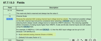
=>Answer:You can find the information from the RT1170RM:
So, it reduces the selected ADC analog channel input voltage level by a factor.
If your SCALE=1, then your input should smaller than the VREFH, otherwise, the pin can't be guaranteed, it maybe damaged.
6. What is the input impedance of VREFH? The only spec I can find in the datasheet is a maximum supply current of 2 mA.
=>Answer: Yes, the datasheet didn't provide the input impedance of VREFH, you can consider it very small and ignore it.
Wish it helps you!
Best Regards,
Kerry
- Mark as New
- Bookmark
- Subscribe
- Mute
- Subscribe to RSS Feed
- Permalink
- Report Inappropriate Content
Hi Kerry,
Thank you very much for answering my questions. It makes a lot of sense that the input voltage would be reduced rather than the reference voltage being increased. Otherwise you wouldn't need to the scaling function because you could just provide a higher VREFH.
I am disappointed to hear that the device may be damaged if the CSCALE option is not turned on and the input is greater than VREFH. I can see how an input voltage greater than NVCC_GPIO would damage the input. The injection current spec is not published, but I know it is very small and it doesn't take much to damage an input.
However once the signal is buffered by the mux, I would hope that the internal circuitry would be able to withstand the overvoltage condition. Of course all voltages greater than VREFH will be converted as full scale. Are you sure that if an input is at 3.3V and CSCALE is not enabled, the A/D converter will be damaged? That means it is possible for a company to release a firmware update that accidentally doesn't enable CSCALE and damage all of their products in the field. That is a very scary thought.
I'm sorry for asking the question again, but it scares me to know that if the software fails to enable CSCALE that the chip could be damaged.
Regards,
Greg
- Mark as New
- Bookmark
- Subscribe
- Mute
- Subscribe to RSS Feed
- Permalink
- Report Inappropriate Content
Hi @gcary ,
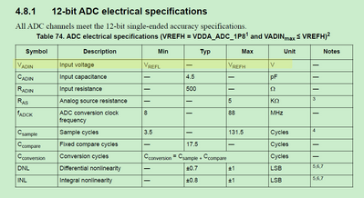
Maybe higher the VREFH damage the pin is not proper description, but from the datasheet, the input pin should follow the datasheet data, eg:
Normally, chip will leave some margin, but, to the chip company, we can't guarantee the feature when the input data is exceed the datasheet's range, that's why I say things heavy, just to protect your chip.
So, If you can't make sure, you can add some external circuits, and make sure the input voltage won't exceed the datasheet's range.
Thanks a lot for your understanding.
Best Regards,
Kerry
- Mark as New
- Bookmark
- Subscribe
- Mute
- Subscribe to RSS Feed
- Permalink
- Report Inappropriate Content
Hi Kerry,
Thank you for your reply. I agree that the datasheet lists the maximum VADIN, but it also does not list a warning if it is exceeded. Assuming there is no damage, VADIN greater than VREFH will result in the max conversion result (0xFFF) for the range of VREFH to VADINmax.
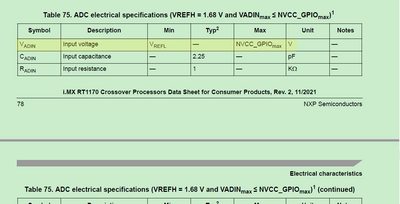
Where does the datasheet say the chip will be damaged? Table 75 says that VADIN can be as high as NVCC_GPIOmax, and there is no mention of CSCALE. I would expect this to be in the Notes column or in the notes below the table if it matters.
I agree with everything you've shown me except for the issue of the chip being damaged. If this is true, then the datasheet should mention it. The datasheet lists the specs over the range of voltages that make sense. For example, would the ENOB specs make any sense if VREFH was 1.68V and CSCALE is not enabled?
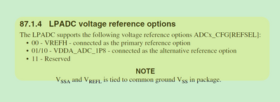
I think tables 74, 75, and 76 in the datasheet need more explanation for what each one covers. In the reference manual in section 87.7.8 (LPADC Configuration Register (CFG)), there are 2 bits for Voltage Reference Selection:
What are these 3 options?
Regards,
Greg
- Mark as New
- Bookmark
- Subscribe
- Mute
- Subscribe to RSS Feed
- Permalink
- Report Inappropriate Content
Hi @gcary ,
Thanks for your updated information.
As I told you, if you exceed the datasheet's range and the RM mentioned situation, the feature can't be guaranteed, chip company datasheet normally don't mention if over the datasheet's range, what's will happen, maybe damange, maybe can't realize the feature. Eg, if the chip vdd just support max 3.8V, you supply 30V or more, it will damage the chip, but datasheet won't mention it, to the application engeer, we need to follow the chip datasheet, just kick out the abnormal factors.
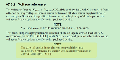
About the reference option, in the RM, it already mention it, as your picture shows, in the :
NOTE: See the chip configuration information on the voltage reference options specific to this packaged
device.
Wish it helps you!
Best Regards,
Kerry
- Mark as New
- Bookmark
- Subscribe
- Mute
- Subscribe to RSS Feed
- Permalink
- Report Inappropriate Content
Thank you Kerry. I understand what you're saying about exceeding the specifications. There is a difference in what I'm trying to point out though. The specification in table 75 says nothing about CSCALE. If I look at that spec, the only thing I would conclude is that the chip will not be damaged if VREFH is 1.62V and VADIN is <= NVCC_GPIOmax. If you require me to read the entire Reference Manual to validate everything in the Datasheet, that is not reasonable. The datasheet should cover this. If indeed the chip will be damaged if CSCALE = 0, then the datasheet needs to specify this. The appropriate place to list this is with a number in the Notes column, referencing a number in the notes below the table. There are 13 notes under table 75. Wouldn't it be appropriate for one of them to say "CSCALE = 0"?
Regards,
Greg
- Mark as New
- Bookmark
- Subscribe
- Mute
- Subscribe to RSS Feed
- Permalink
- Report Inappropriate Content
Hi @gcary ,
Thanks for your updated information.
I totally understand you! Even to me, I also normally check the datasheet, and the RM together. You are right, the doc is not Perfect, sometimes, even have bugs.
So, to our application engineer, normally we need to read the related document together to familiar the chip.
To the RT chip, normally, RT RM is also very important, it will put some note in the module chapter, instead of the datasheet directly.
Anyway, if you meet any issues, just kindly let me know, we will help you to confirm it.
To this ADC input voltage, please still follow: if full scale, follow the datasheet range, if using CSCALE =0, then make sure input not larger than 3.3V.
Best Regards,
Kerry
- Mark as New
- Bookmark
- Subscribe
- Mute
- Subscribe to RSS Feed
- Permalink
- Report Inappropriate Content
Hi Kerry,
I'm glad you understand. But I am surprised that you did not say that you will submit a request to change the documentation. There are 6,214 pages in the Reference Manual. It is unacceptable to expect a customer to read all of those pages in order to know if they are violating an electrical specification of the chip. The datasheet should cover every electrical specification of the chip. In this case it is even worse than having to read all of those pages. I would also have to make the connection that I would damage the chip if the CSCALE bit is not set to 0.
Thank you for answering my questions.
Regards,
Greg
- Mark as New
- Bookmark
- Subscribe
- Mute
- Subscribe to RSS Feed
- Permalink
- Report Inappropriate Content
Hi @gcary ,
Yes, of course!
I will post the request to add the CSCALE information in the datasheet to the internal related team.
Best Regards,
Kerry
- Mark as New
- Bookmark
- Subscribe
- Mute
- Subscribe to RSS Feed
- Permalink
- Report Inappropriate Content
Thank you very much for your help on this topic. I appreciate your willingness to discuss this with me. Hopefully I won't have more questions!
Regards,
Greg
- Mark as New
- Bookmark
- Subscribe
- Mute
- Subscribe to RSS Feed
- Permalink
- Report Inappropriate Content
I'm sorry, I forgot to thank you for showing me the table that defines the VREF options!
Greg
