- NXP Forums
- Product Forums
- General Purpose MicrocontrollersGeneral Purpose Microcontrollers
- i.MX Forumsi.MX Forums
- QorIQ Processing PlatformsQorIQ Processing Platforms
- Identification and SecurityIdentification and Security
- Power ManagementPower Management
- MCX Microcontrollers
- S32G
- S32K
- S32V
- MPC5xxx
- Other NXP Products
- Wireless Connectivity
- S12 / MagniV Microcontrollers
- Powertrain and Electrification Analog Drivers
- Sensors
- Vybrid Processors
- Digital Signal Controllers
- 8-bit Microcontrollers
- ColdFire/68K Microcontrollers and Processors
- PowerQUICC Processors
- OSBDM and TBDML
-
- Solution Forums
- Software Forums
- MCUXpresso Software and ToolsMCUXpresso Software and Tools
- CodeWarriorCodeWarrior
- MQX Software SolutionsMQX Software Solutions
- Model-Based Design Toolbox (MBDT)Model-Based Design Toolbox (MBDT)
- FreeMASTER
- eIQ Machine Learning Software
- Embedded Software and Tools Clinic
- S32 SDK
- S32 Design Studio
- Vigiles
- GUI Guider
- Zephyr Project
- Voice Technology
- Application Software Packs
- Secure Provisioning SDK (SPSDK)
- Processor Expert Software
-
- Topics
- Mobile Robotics - Drones and RoversMobile Robotics - Drones and Rovers
- NXP Training ContentNXP Training Content
- University ProgramsUniversity Programs
- Rapid IoT
- NXP Designs
- SafeAssure-Community
- OSS Security & Maintenance
- Using Our Community
-
-
- Home
- :
- i.MX Forums
- :
- i.MX RT
- :
- Re: RT1064 with non-cacheable are in HyperRAM problem
RT1064 with non-cacheable area in HyperRAM problem
- Subscribe to RSS Feed
- Mark Topic as New
- Mark Topic as Read
- Float this Topic for Current User
- Bookmark
- Subscribe
- Mute
- Printer Friendly Page
RT1064 with non-cacheable area in HyperRAM problem
- Mark as New
- Bookmark
- Subscribe
- Mute
- Subscribe to RSS Feed
- Permalink
- Report Inappropriate Content
I have a system with a RT1064 and HyperRAM (same chip as EVK). This works perfectly, I have run RAM tests for weeks and weeks, all checks out fine.
But, if I place the non-cacheable area in the HyperRAM, things go downhill quickly.....I get hardfaults (and sometimes debugger "dies" when debugging). I have been working with this for some days now, and it seems that the triggering factor is if one of the following is true:
a) The whole 8 MByte of HyperRAM is defined as non-cacheable in the MPU (buffered, non-cacheable)
or
b) The last part of HyperRAM (2 MByte) is defined as non-cacheable
Now, in case of b), if I just move the non-cacheable are to some other place like OCRAM2, all is ok (and all other data is in the first 6 MByte of HyperRAM).
So, it seems that if the HyperRAM or part of the HyperRAM is set as non-cacheable and that part is used, I will get hardfaults.
I have a identical system with SDRAM, and there the same application behaves as expected, I can place the non-cacheable area at the end of SDRAM, and all works perfect.
Are there any problem in placing non-cached data in HyperRAM (or am I fighting something else) ??
- Mark as New
- Bookmark
- Subscribe
- Mute
- Subscribe to RSS Feed
- Permalink
- Report Inappropriate Content
Gonna bump this as I have found the same thing.
Indeed globally disabling cache with SCB_DisableDCache() also resulted in similar, but not exactly the same behaviour. Basically as described above I'd see memory management faults here there and everywhere. It'll work for a short time, but eventually except somewhere.
I wonder if it could because with cache on, all transactions would be aligned? But with cache off we get a bunch of ad-hoc transactions?
I'm doing this to test the memory, as we've been finding the very occasional crash on some devices where we see corrupt data.
- Mark as New
- Bookmark
- Subscribe
- Mute
- Subscribe to RSS Feed
- Permalink
- Report Inappropriate Content
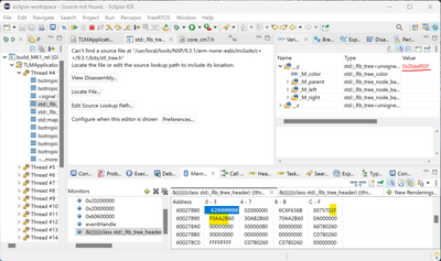
This is very curious:
Misaligned read, it would seem, causing an exception.
It's also repeatable.
- Mark as New
- Bookmark
- Subscribe
- Mute
- Subscribe to RSS Feed
- Permalink
- Report Inappropriate Content
Hi Carsten,
I'm checking this internally. I'll provide you an update as soon as possible.
Regards,
Victor
- Mark as New
- Bookmark
- Subscribe
- Mute
- Subscribe to RSS Feed
- Permalink
- Report Inappropriate Content
- Mark as New
- Bookmark
- Subscribe
- Mute
- Subscribe to RSS Feed
- Permalink
- Report Inappropriate Content
Hi Carsten,
Thanks for your patience with this case. I received a response from the applications team. They have some follow-up questions for you.
I'm not aware of a reason HyperRAM can't be used with FlexSPI and non-cacheable policy. But maybe there is an issue with how the project is configuring this. It would be helpful to get the .MAP file from the linker when the NonCacheable region is moved to HyperRAM, so we can see how the linker is set up for the NonCacheable memory in the project.
Are the hard faults/debugger crashes occurring before or after main()? If the issues are occurring after main(), at what point do the issues start in the application? And how does that relate to the data placed in HyperRAM?
And are there cacheable regions in HyperRAM, and does the application work fine using them? I'm trying to understand if the issue is specific to non-cacheable regions, or to any linker regions in HyperRAM.
Regards,
Victor
- Mark as New
- Bookmark
- Subscribe
- Mute
- Subscribe to RSS Feed
- Permalink
- Report Inappropriate Content
Hi Victor,
I tried to do some more testing with regards to your questions.
What I did was modifying the scatterfile:
Here the non-cachable is located at the top 2 MB in the HyperRAM, this does not work:
#define m_ncache_start 0x60600000 // End of HyperRAM minus 2 MByte
#define m_ncache_size 0x00200000 // 2 MByte for non-chachable memory
If I place the non-cacheable area in OCRAM2 like this:
#define m_ncache_start 0x202A0000 // End of OCRAM2 minus 128 KByte
#define m_ncache_size 0x00020000 // 128 KByte for non-chachable memory
it works perfectly. I debugged the code thru the setting of the MPU for the non-cache area, in both cases the parameters were set correctly (address and area).
The rest (6 MB) of the HyperRAM is set as cachable etc and is working perfectly fine as "normal memory". I use the SystemInitHook() to initialize the HyperRAM (MSP is placed in DTCM) so that scatterloading etc will work with initialized HyperRAM interface. All this is working fine.
In main(), I then start USB support (CDC), and then it hangs in the USB_DeviceSetSpeed() function.
It continues to loop in:
while (ptr1 < ptr2) {
}
The g_UsbDeviceConfigurationDescriptor are located in the non-cache area, so I suspect this has something to do with it (again, if I place the non-cache in OCRAM2 it runs without problems)
If I disable the USB, and run some of my own code (CMSIS RTOS2 etc), just a simple sprintf from a variable that are located in the non-cached area results in a BusFault (imprecise)
If I place (for example) the stacks for the threads I start, in the non-cachable area, I get a busfault as soon as the thread starts to run (also Busfault, imprecise).
I have included 2 (partial) map files, one where USB is included, and 1 where it is not included (not calling init function) and the scatterfile.
I'm a little lost, I can't completely rule out that I'm doing something wrong, I just have hard time seeing it....
- Mark as New
- Bookmark
- Subscribe
- Mute
- Subscribe to RSS Feed
- Permalink
- Report Inappropriate Content
Hello Carsten,
Thanks for the additional information! I already passed this to the applications team. I will give you an update as soon as possible.
Regards,
Victor
- Mark as New
- Bookmark
- Subscribe
- Mute
- Subscribe to RSS Feed
- Permalink
- Report Inappropriate Content
Thanks Victor,
one thing that crossed my mind....
In AN12239 (https://www.nxp.com/docs/en/nxp/application-notes/AN12239.pdf), there is a list of validated HyperRAM devices:
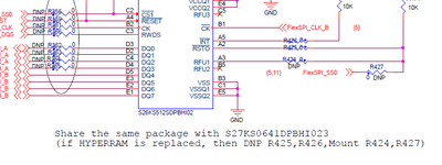
I see that the 7KS0641DPHI02 is listed as FAIL ! This is the part I use, and as I understand it, also the part suggested in the schematics for the 1064 EVK:
Because of that, I assembled another prototype with the S27KS0642GABHV020 (https://www.cypress.com/file/498611/download) instead.
For some reason (could be the assembly of the prototype) the HyperRAM is not working at all (garbage read from it). Just to be sure, can you confirm that the S27KS0642GABHV020 will be able to use the same LUT, setup etc, as the 7KS0641DPHI02 ?
I see the 0641 is listed as "HyperRAM 1.0" and the 0642 is listed as "HyperRAM 2.0"
My setup is as follows:
Pin config:
// HyperRAM
IOMUXC_SetPinMux(
IOMUXC_GPIO_SD_B1_00_FLEXSPIB_DATA03, /* GPIO_SD_B1_00 is configured as FLEXSPIB_DATA03 */
1U); /* Software Input On Field: Force input path of pad GPIO_SD_B1_00 */
IOMUXC_SetPinMux(
IOMUXC_GPIO_SD_B1_01_FLEXSPIB_DATA02, /* GPIO_SD_B1_01 is configured as FLEXSPIB_DATA02 */
1U); /* Software Input On Field: Force input path of pad GPIO_SD_B1_01 */
IOMUXC_SetPinMux(
IOMUXC_GPIO_SD_B1_02_FLEXSPIB_DATA01, /* GPIO_SD_B1_02 is configured as FLEXSPIB_DATA01 */
1U); /* Software Input On Field: Force input path of pad GPIO_SD_B1_02 */
IOMUXC_SetPinMux(
IOMUXC_GPIO_SD_B1_03_FLEXSPIB_DATA00, /* GPIO_SD_B1_03 is configured as FLEXSPIB_DATA00 */
1U); /* Software Input On Field: Force input path of pad GPIO_SD_B1_03 */
IOMUXC_SetPinMux(
IOMUXC_GPIO_SD_B1_04_FLEXSPIB_SCLK, /* GPIO_SD_B1_04 is configured as FLEXSPIB_SCLK */
1U); /* Software Input On Field: Force input path of pad GPIO_SD_B1_04 */
IOMUXC_SetPinMux(
IOMUXC_GPIO_SD_B1_05_FLEXSPIA_DQS, /* GPIO_SD_B1_05 is configured as FLEXSPIA_DQS */
1U); /* Software Input On Field: Force input path of pad GPIO_SD_B1_05 */
IOMUXC_SetPinMux(
IOMUXC_GPIO_SD_B1_06_FLEXSPIA_SS0_B, /* GPIO_SD_B1_06 is configured as FLEXSPIA_SS0_B */
1U); /* Software Input On Field: Force input path of pad GPIO_SD_B1_06 */
IOMUXC_SetPinMux(
IOMUXC_GPIO_SD_B1_07_FLEXSPIA_SCLK, /* GPIO_SD_B1_07 is configured as FLEXSPIA_SCLK */
1U); /* Software Input On Field: Force input path of pad GPIO_SD_B1_07 */
IOMUXC_SetPinMux(
IOMUXC_GPIO_SD_B1_08_FLEXSPIA_DATA00, /* GPIO_SD_B1_08 is configured as FLEXSPIA_DATA00 */
1U); /* Software Input On Field: Force input path of pad GPIO_SD_B1_08 */
IOMUXC_SetPinMux(
IOMUXC_GPIO_SD_B1_09_FLEXSPIA_DATA01, /* GPIO_SD_B1_09 is configured as FLEXSPIA_DATA01 */
1U); /* Software Input On Field: Force input path of pad GPIO_SD_B1_09 */
IOMUXC_SetPinMux(
IOMUXC_GPIO_SD_B1_10_FLEXSPIA_DATA02, /* GPIO_SD_B1_10 is configured as FLEXSPIA_DATA02 */
1U); /* Software Input On Field: Force input path of pad GPIO_SD_B1_10 */
IOMUXC_SetPinMux(
IOMUXC_GPIO_SD_B1_11_FLEXSPIA_DATA03, /* GPIO_SD_B1_11 is configured as FLEXSPIA_DATA03 */
1U); /* Software Input On Field: Force input path of pad GPIO_SD_B1_11 */
IOMUXC_SetPinConfig(
IOMUXC_GPIO_SD_B1_00_FLEXSPIB_DATA03, /* GPIO_SD_B1_00 PAD functional properties : */
0x10F1u); /* Slew Rate Field: Fast Slew Rate
Drive Strength Field: R0/6
Speed Field: max(200MHz)
Open Drain Enable Field: Open Drain Disabled
Pull / Keep Enable Field: Pull/Keeper Enabled
Pull / Keep Select Field: Keeper
Pull Up / Down Config. Field: 100K Ohm Pull Down
Hyst. Enable Field: Hysteresis Disabled */
IOMUXC_SetPinConfig(
IOMUXC_GPIO_SD_B1_01_FLEXSPIB_DATA02, /* GPIO_SD_B1_01 PAD functional properties : */
0x10F1u); /* Slew Rate Field: Fast Slew Rate
Drive Strength Field: R0/6
Speed Field: max(200MHz)
Open Drain Enable Field: Open Drain Disabled
Pull / Keep Enable Field: Pull/Keeper Enabled
Pull / Keep Select Field: Keeper
Pull Up / Down Config. Field: 100K Ohm Pull Down
Hyst. Enable Field: Hysteresis Disabled */
IOMUXC_SetPinConfig(
IOMUXC_GPIO_SD_B1_02_FLEXSPIB_DATA01, /* GPIO_SD_B1_02 PAD functional properties : */
0x10F1u); /* Slew Rate Field: Fast Slew Rate
Drive Strength Field: R0/6
Speed Field: max(200MHz)
Open Drain Enable Field: Open Drain Disabled
Pull / Keep Enable Field: Pull/Keeper Enabled
Pull / Keep Select Field: Keeper
Pull Up / Down Config. Field: 100K Ohm Pull Down
Hyst. Enable Field: Hysteresis Disabled */
IOMUXC_SetPinConfig(
IOMUXC_GPIO_SD_B1_03_FLEXSPIB_DATA00, /* GPIO_SD_B1_03 PAD functional properties : */
0x10F1u); /* Slew Rate Field: Fast Slew Rate
Drive Strength Field: R0/6
Speed Field: max(200MHz)
Open Drain Enable Field: Open Drain Disabled
Pull / Keep Enable Field: Pull/Keeper Enabled
Pull / Keep Select Field: Keeper
Pull Up / Down Config. Field: 100K Ohm Pull Down
Hyst. Enable Field: Hysteresis Disabled */
IOMUXC_SetPinConfig(
IOMUXC_GPIO_SD_B1_04_FLEXSPIB_SCLK, /* GPIO_SD_B1_04 PAD functional properties : */
0x10F1u); /* Slew Rate Field: Fast Slew Rate
Drive Strength Field: R0/6
Speed Field: max(200MHz)
Open Drain Enable Field: Open Drain Disabled
Pull / Keep Enable Field: Pull/Keeper Enabled
Pull / Keep Select Field: Keeper
Pull Up / Down Config. Field: 100K Ohm Pull Down
Hyst. Enable Field: Hysteresis Disabled */
IOMUXC_SetPinConfig(
IOMUXC_GPIO_SD_B1_05_FLEXSPIA_DQS, /* GPIO_SD_B1_05 PAD functional properties : */
0x0130F1u); /* Slew Rate Field: Fast Slew Rate
Drive Strength Field: R0/6
Speed Field: max(200MHz)
Open Drain Enable Field: Open Drain Disabled
Pull / Keep Enable Field: Pull/Keeper Enabled
Pull / Keep Select Field: Pull
Pull Up / Down Config. Field: 100K Ohm Pull Down
Hyst. Enable Field: Hysteresis Enabled */
IOMUXC_SetPinConfig(
IOMUXC_GPIO_SD_B1_06_FLEXSPIA_SS0_B, /* GPIO_SD_B1_06 PAD functional properties : */
0x10F1u); /* Slew Rate Field: Fast Slew Rate
Drive Strength Field: R0/6
Speed Field: max(200MHz)
Open Drain Enable Field: Open Drain Disabled
Pull / Keep Enable Field: Pull/Keeper Enabled
Pull / Keep Select Field: Keeper
Pull Up / Down Config. Field: 100K Ohm Pull Down
Hyst. Enable Field: Hysteresis Disabled */
IOMUXC_SetPinConfig(
IOMUXC_GPIO_SD_B1_07_FLEXSPIA_SCLK, /* GPIO_SD_B1_07 PAD functional properties : */
0x10F1u); /* Slew Rate Field: Fast Slew Rate
Drive Strength Field: R0/6
Speed Field: max(200MHz)
Open Drain Enable Field: Open Drain Disabled
Pull / Keep Enable Field: Pull/Keeper Enabled
Pull / Keep Select Field: Keeper
Pull Up / Down Config. Field: 100K Ohm Pull Down
Hyst. Enable Field: Hysteresis Disabled */
IOMUXC_SetPinConfig(
IOMUXC_GPIO_SD_B1_08_FLEXSPIA_DATA00, /* GPIO_SD_B1_08 PAD functional properties : */
0x10F1u); /* Slew Rate Field: Fast Slew Rate
Drive Strength Field: R0/6
Speed Field: max(200MHz)
Open Drain Enable Field: Open Drain Disabled
Pull / Keep Enable Field: Pull/Keeper Enabled
Pull / Keep Select Field: Keeper
Pull Up / Down Config. Field: 100K Ohm Pull Down
Hyst. Enable Field: Hysteresis Disabled */
IOMUXC_SetPinConfig(
IOMUXC_GPIO_SD_B1_09_FLEXSPIA_DATA01, /* GPIO_SD_B1_09 PAD functional properties : */
0x10F1u); /* Slew Rate Field: Fast Slew Rate
Drive Strength Field: R0/6
Speed Field: max(200MHz)
Open Drain Enable Field: Open Drain Disabled
Pull / Keep Enable Field: Pull/Keeper Enabled
Pull / Keep Select Field: Keeper
Pull Up / Down Config. Field: 100K Ohm Pull Down
Hyst. Enable Field: Hysteresis Disabled */
IOMUXC_SetPinConfig(
IOMUXC_GPIO_SD_B1_10_FLEXSPIA_DATA02, /* GPIO_SD_B1_10 PAD functional properties : */
0x10F1u); /* Slew Rate Field: Fast Slew Rate
Drive Strength Field: R0/6
Speed Field: max(200MHz)
Open Drain Enable Field: Open Drain Disabled
Pull / Keep Enable Field: Pull/Keeper Enabled
Pull / Keep Select Field: Keeper
Pull Up / Down Config. Field: 100K Ohm Pull Down
Hyst. Enable Field: Hysteresis Disabled */
IOMUXC_SetPinConfig(
IOMUXC_GPIO_SD_B1_11_FLEXSPIA_DATA03, /* GPIO_SD_B1_11 PAD functional properties : */
0x10F1u); /* Slew Rate Field: Fast Slew Rate
Drive Strength Field: R0/6
Speed Field: max(200MHz)
Open Drain Enable Field: Open Drain Disabled
Pull / Keep Enable Field: Pull/Keeper Enabled
Pull / Keep Select Field: Keeper
Pull Up / Down Config. Field: 100K Ohm Pull Down
Hyst. Enable Field: Hysteresis Disabled */
//
Init function:
void initHyperRAM(void) {

	// Keep the customLUT and the deviceconfig strcutures and their init values local to this function as we are called
	// from SystemInit() and this is before C runtime init has been called. By keeping the structures local, the prolog of the function will
	// take care of the init of the values instead of the C runtime initialization code :)

	uint32_t customLUT[20] = {
        // Read Data
        [4 * HYPERRAM_CMD_LUT_SEQ_IDX_READDATA] =
            FLEXSPI_LUT_SEQ(kFLEXSPI_Command_DDR, kFLEXSPI_8PAD, 0xA0, kFLEXSPI_Command_RADDR_DDR, kFLEXSPI_8PAD, 0x18),
        [4 * HYPERRAM_CMD_LUT_SEQ_IDX_READDATA + 1] = FLEXSPI_LUT_SEQ(
            kFLEXSPI_Command_CADDR_DDR, kFLEXSPI_8PAD, 0x10, kFLEXSPI_Command_DUMMY_RWDS_DDR, kFLEXSPI_8PAD, 0x06),
        [4 * HYPERRAM_CMD_LUT_SEQ_IDX_READDATA + 2] =
            FLEXSPI_LUT_SEQ(kFLEXSPI_Command_READ_DDR, kFLEXSPI_8PAD, 0x04, kFLEXSPI_Command_STOP, kFLEXSPI_1PAD, 0x00),

        // Write Data
        [4 * HYPERRAM_CMD_LUT_SEQ_IDX_WRITEDATA] =
            FLEXSPI_LUT_SEQ(kFLEXSPI_Command_DDR, kFLEXSPI_8PAD, 0x20, kFLEXSPI_Command_RADDR_DDR, kFLEXSPI_8PAD, 0x18),
        [4 * HYPERRAM_CMD_LUT_SEQ_IDX_WRITEDATA + 1] = FLEXSPI_LUT_SEQ(
            kFLEXSPI_Command_CADDR_DDR, kFLEXSPI_8PAD, 0x10, kFLEXSPI_Command_DUMMY_RWDS_DDR, kFLEXSPI_8PAD, 0x06),
        [4 * HYPERRAM_CMD_LUT_SEQ_IDX_WRITEDATA + 2] = FLEXSPI_LUT_SEQ(
            kFLEXSPI_Command_WRITE_DDR, kFLEXSPI_8PAD, 0x04, kFLEXSPI_Command_STOP, kFLEXSPI_1PAD, 0x00),

        // Read Register
        [4 * HYPERRAM_CMD_LUT_SEQ_IDX_READREG] =
            FLEXSPI_LUT_SEQ(kFLEXSPI_Command_DDR, kFLEXSPI_8PAD, 0xE0, kFLEXSPI_Command_RADDR_DDR, kFLEXSPI_8PAD, 0x18),
        [4 * HYPERRAM_CMD_LUT_SEQ_IDX_READREG + 1] = FLEXSPI_LUT_SEQ(
            kFLEXSPI_Command_CADDR_DDR, kFLEXSPI_8PAD, 0x10, kFLEXSPI_Command_DUMMY_RWDS_DDR, kFLEXSPI_8PAD, 0x06),
        [4 * HYPERRAM_CMD_LUT_SEQ_IDX_READREG + 2] =
            FLEXSPI_LUT_SEQ(kFLEXSPI_Command_READ_DDR, kFLEXSPI_8PAD, 0x04, kFLEXSPI_Command_STOP, kFLEXSPI_1PAD, 0x00),

        // Write Register
        [4 * HYPERRAM_CMD_LUT_SEQ_IDX_WRITEREG] =
            FLEXSPI_LUT_SEQ(kFLEXSPI_Command_DDR, kFLEXSPI_8PAD, 0x60, kFLEXSPI_Command_RADDR_DDR, kFLEXSPI_8PAD, 0x18),
        [4 * HYPERRAM_CMD_LUT_SEQ_IDX_WRITEREG + 1] = FLEXSPI_LUT_SEQ(
            kFLEXSPI_Command_CADDR_DDR, kFLEXSPI_8PAD, 0x10, kFLEXSPI_Command_DUMMY_RWDS_DDR, kFLEXSPI_8PAD, 0x06),
        [4 * HYPERRAM_CMD_LUT_SEQ_IDX_WRITEREG + 2] = FLEXSPI_LUT_SEQ(
            kFLEXSPI_Command_WRITE_DDR, kFLEXSPI_8PAD, 0x04, kFLEXSPI_Command_STOP, kFLEXSPI_1PAD, 0x00),
	};


	flexspi_device_config_t deviceconfig = {
		//.flexspiRootClk = 332000000, // 332MHZ SPI serial clock, set later on
		.isSck2Enabled = false,
		.flashSize = FLASH_SIZE,
		.CSIntervalUnit = kFLEXSPI_CsIntervalUnit1SckCycle,
		.CSInterval = 2,
		.CSHoldTime = 0,
		.CSSetupTime = 4,
		.dataValidTime = 1,
		.columnspace = 3,
		.enableWordAddress = true,
		.AWRSeqIndex = HYPERRAM_CMD_LUT_SEQ_IDX_WRITEDATA,
		.AWRSeqNumber = 1,
		.ARDSeqIndex = HYPERRAM_CMD_LUT_SEQ_IDX_READDATA,
		.ARDSeqNumber = 1,
		.AHBWriteWaitUnit = kFLEXSPI_AhbWriteWaitUnit2AhbCycle,
		.AHBWriteWaitInterval = 0,
		.enableWriteMask = true,
	};


	initPins();

	flexspi_config_t config;

	volatile int xx=0;
	for (xx=0; xx<1000000; xx++)
	;


	__disable_irq();

    // For XIP targets, change to use PLL2 PFD2 instead of re-configuring PLL3 PFD0 to prevent the potential impact to FLEXSPI2
    CLOCK_InitSysPfd(kCLOCK_Pfd2, 29);    // Set PLL2 PFD2 clock 328MHZ
    CLOCK_SetMux(kCLOCK_FlexspiMux, 0x2); // Choose PLL2 PFD2 clock as flexspi source clock
    CLOCK_SetDiv(kCLOCK_FlexspiDiv, 0);   // flexspi clock 328M

    // Get FLEXSPI default settings and configure the flexspi
    FLEXSPI_GetDefaultConfig(&config);

    // Init FLEXSPI
    config.rxSampleClock = kFLEXSPI_ReadSampleClkExternalInputFromDqsPad;
    config.enableSckBDiffOpt = true;
    config.enableCombination = true;
    config.ahbConfig.enableAHBPrefetch = true;
    config.ahbConfig.enableAHBBufferable = true;
    config.ahbConfig.enableAHBCachable = true;

	FLEXSPI_Init(EXAMPLE_FLEXSPI, &config);

	// Get FlexSPI clock frequency. The frquency output on SCLK A/B will be half of this as we run DDR
	deviceconfig.flexspiRootClk=flexspi_get_frequency();
    // Configure RAM settings according to serial RAM feature
    FLEXSPI_SetFlashConfig(EXAMPLE_FLEXSPI, &deviceconfig, kFLEXSPI_PortA1);

    // Update LUT table
    FLEXSPI_UpdateLUT(EXAMPLE_FLEXSPI, 0, customLUT, ARRAY_SIZE(customLUT));

    // Do software reset
    FLEXSPI_SoftwareReset(EXAMPLE_FLEXSPI);

	__enable_irq();
}
Now, I dont know if the 0642 versus the 0641 device could have anything at all to say regarding my non-cache issue I see (I doubt it very much), but I thought that I would investigate....
- Mark as New
- Bookmark
- Subscribe
- Mute
- Subscribe to RSS Feed
- Permalink
- Report Inappropriate Content
Hello Carsten,
The reason why we mention that with the 7KS0641 the test failed is related to some issues with chip select timing on Gen1 Cypress HyperRAM. The issue has been fixed in their Gen 2 devices. In the part numbers, the digit after the density reflects the device technology generation. So 7KS0641 devices have the problem, but 7KS0642 devices do not. So as far as I can tell, you shouldn't have any problems migrating from one HyperRAM to another. However, it would be better if you contact directly the manufacturer. They will have more information regarding the implications of one memory being HyperRAM 1.0 and the other 2.0.
I'm still investigating internally with the apps team the implications of having the non_cacheble section at the HyperRAM. I will give you an update as soon as possible.
Regards,
Victor
- Mark as New
- Bookmark
- Subscribe
- Mute
- Subscribe to RSS Feed
- Permalink
- Report Inappropriate Content
Hello Carsten,
Can we get the source code configuring the MPU, as shown below?
MPU code:
/* Region 7 setting: Memory with Normal type, not shareable, outer/inner write back */
MPU->RBAR = ARM_MPU_RBAR(7, 0x80000000U);
MPU->RASR = ARM_MPU_RASR(0, ARM_MPU_AP_FULL, 0, 0, 1, 1, 0, ARM_MPU_REGION_SIZE_32MB);
/* Region 8 setting, set last 2MB of SDRAM can't be accessed by cache, glocal variables which are not expected to be
* accessed by cache can be put here */
/* Memory with Normal type, not shareable, non-cacheable */
MPU->RBAR = ARM_MPU_RBAR(8, 0x81E00000U);
MPU->RASR = ARM_MPU_RASR(0, ARM_MPU_AP_FULL, 1, 0, 0, 0, 0, ARM_MPU_REGION_SIZE_2MB);
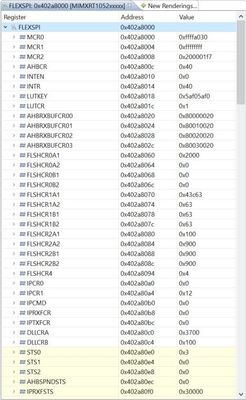
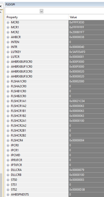
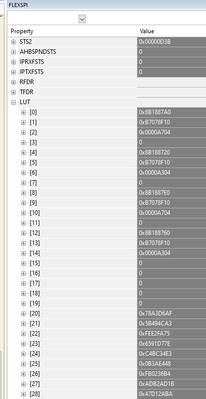
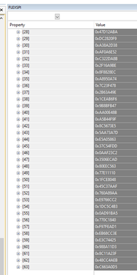
While we are doing that, can we also get a capture of the FlexSPI registers after these hard faults, from the debugger similar to the screenshot below? Perhaps the interrupt or status flags will enlighten us.
While I see no issue configuring non-cacheable memory in HyperRAM, I do want to comment on the application using this. The external memory performance with cache disabled will be substantially slower. I would carefully consider how to use it in the application.
For example, using with USB is mentioned. Sharing RAM between multiple masters in the MCU does require a non-cacheable region since the cache is only used by the core. So the USB endpoint buffers or any RAM updated by a master other than the core should be non-cacheable. Ideally, the internal OCRAM would be used for these shared RAMs, as it is much higher performance than external memory. In particular with high-speed USB, or any master that requires high performance from the RAM, using slower external RAM may lead to some bandwidth/latency issues. Usually, these shared RAMs with other masters are small size and ideal for placing in internal OCRAM.
Also, thread stacks were mentioned placing in non-cacheable HyperRAM. Since stacks are used all the time, and frequently non-linear accesses, storing in non-cached external memory will likely have a major impact on the performance of the application. The stacks are used only by the core master. Ideally, stacks would be placed in DTCM. Or if they don't fit in DTCM, then using cached OCRAM or external memory would optimize performance.
But regardless of how the application uses the memory, we should be able to enable non-cacheable regions in HyperRAM.
Regards,
Victor
- Mark as New
- Bookmark
- Subscribe
- Mute
- Subscribe to RSS Feed
- Permalink
- Report Inappropriate Content
Hi Victor,
Thanks for sticking with me on this one
I know that it is a bad idea to place stacks etc. in non-cached memory, no doubt about that!
The reason I found this problem in the first place is because I have made several testboards for RT1064, one with SDRAM and one with HyperRAM (also doing SDRAM testing on LPC54628). On these, I run different tests, one of them is Dhrystone, this is to get an idea of the penalty running code/data in the different sections/types of memory for coming projects.
Now, I mentioned that the 7KS0641 was suggested on the EVK schematics (hence I used that in my design), and in the AN it was mentioned that the '0641 would fail. I used the '0642 instead, and that would not run (at least with the same parameters as the '0641 did).
Then I looked in the application note "Migrating from S27KL0641/S27KS0641 to S27KL0642/S27KS0642" from Cypress:
https://www.cypress.com/file/498626/download
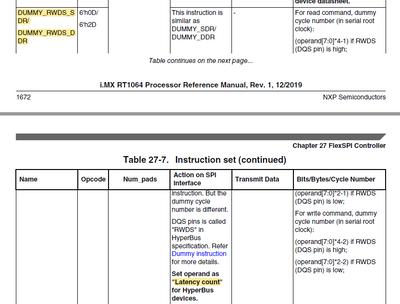
There they mention one "critical difference", that is the "Default latency" which is 6 for the '0641 and 7 for the '0642. I found that this latency is set in the LUT for each command:
So I changed the LUT:
	uint32_t customLUT[20] = {
        // Read Data
        [4 * HYPERRAM_CMD_LUT_SEQ_IDX_READDATA] =
            FLEXSPI_LUT_SEQ(kFLEXSPI_Command_DDR, kFLEXSPI_8PAD, 0xA0, kFLEXSPI_Command_RADDR_DDR, kFLEXSPI_8PAD, 0x18),
        [4 * HYPERRAM_CMD_LUT_SEQ_IDX_READDATA + 1] = FLEXSPI_LUT_SEQ(
            kFLEXSPI_Command_CADDR_DDR, kFLEXSPI_8PAD, 0x10, kFLEXSPI_Command_DUMMY_RWDS_DDR, kFLEXSPI_8PAD, /* 0x06 */ 0x07),
        [4 * HYPERRAM_CMD_LUT_SEQ_IDX_READDATA + 2] =
            FLEXSPI_LUT_SEQ(kFLEXSPI_Command_READ_DDR, kFLEXSPI_8PAD, 0x04, kFLEXSPI_Command_STOP, kFLEXSPI_1PAD, 0x00),

        // Write Data
        [4 * HYPERRAM_CMD_LUT_SEQ_IDX_WRITEDATA] =
            FLEXSPI_LUT_SEQ(kFLEXSPI_Command_DDR, kFLEXSPI_8PAD, 0x20, kFLEXSPI_Command_RADDR_DDR, kFLEXSPI_8PAD, 0x18),
        [4 * HYPERRAM_CMD_LUT_SEQ_IDX_WRITEDATA + 1] = FLEXSPI_LUT_SEQ(
            kFLEXSPI_Command_CADDR_DDR, kFLEXSPI_8PAD, 0x10, kFLEXSPI_Command_DUMMY_RWDS_DDR, kFLEXSPI_8PAD, /* 0x06 */ 0x07),
        [4 * HYPERRAM_CMD_LUT_SEQ_IDX_WRITEDATA + 2] = FLEXSPI_LUT_SEQ(
            kFLEXSPI_Command_WRITE_DDR, kFLEXSPI_8PAD, 0x04, kFLEXSPI_Command_STOP, kFLEXSPI_1PAD, 0x00),

        // Read Register
        [4 * HYPERRAM_CMD_LUT_SEQ_IDX_READREG] =
            FLEXSPI_LUT_SEQ(kFLEXSPI_Command_DDR, kFLEXSPI_8PAD, 0xE0, kFLEXSPI_Command_RADDR_DDR, kFLEXSPI_8PAD, 0x18),
        [4 * HYPERRAM_CMD_LUT_SEQ_IDX_READREG + 1] = FLEXSPI_LUT_SEQ(
            kFLEXSPI_Command_CADDR_DDR, kFLEXSPI_8PAD, 0x10, kFLEXSPI_Command_DUMMY_RWDS_DDR, kFLEXSPI_8PAD, /* 0x06 */ 0x07),
        [4 * HYPERRAM_CMD_LUT_SEQ_IDX_READREG + 2] =
            FLEXSPI_LUT_SEQ(kFLEXSPI_Command_READ_DDR, kFLEXSPI_8PAD, 0x04, kFLEXSPI_Command_STOP, kFLEXSPI_1PAD, 0x00),

        // Write Register
        [4 * HYPERRAM_CMD_LUT_SEQ_IDX_WRITEREG] =
            FLEXSPI_LUT_SEQ(kFLEXSPI_Command_DDR, kFLEXSPI_8PAD, 0x60, kFLEXSPI_Command_RADDR_DDR, kFLEXSPI_8PAD, 0x18),
        [4 * HYPERRAM_CMD_LUT_SEQ_IDX_WRITEREG + 1] = FLEXSPI_LUT_SEQ(
            kFLEXSPI_Command_CADDR_DDR, kFLEXSPI_8PAD, 0x10, kFLEXSPI_Command_DUMMY_RWDS_DDR, kFLEXSPI_8PAD, /* 0x06 */ 0x07),
        [4 * HYPERRAM_CMD_LUT_SEQ_IDX_WRITEREG + 2] = FLEXSPI_LUT_SEQ(
            kFLEXSPI_Command_WRITE_DDR, kFLEXSPI_8PAD, 0x04, kFLEXSPI_Command_STOP, kFLEXSPI_1PAD, 0x00),
	};
This made the '0642 device work! It will now pass my memory test for hours, just like the '0641 device did.
However, no change in the "non-cachable" behavior (as expected I guess)...
So, placing the non-cached area in HyperRAM still fails.
I tried to capture the FlexSPI1 registers right after the (bus) fault:
The MPU is currently set like this:
//----------------------------------------------------------------------------
//
//----------------------------------------------------------------------------
void BOARD_ConfigMPU(void) {
    extern uint32_t Image$$RW_m_ncache$$Base[];
    /* RW_m_ncache_unused is a auxiliary region which is used to get the whole size of noncache section */
    extern uint32_t Image$$RW_m_ncache_unused$$Base[];
    extern uint32_t Image$$RW_m_ncache_unused$$ZI$$Limit[];
    uint32_t nonCacheStart = (uint32_t)Image$$RW_m_ncache$$Base;
    uint32_t size          = ((uint32_t)Image$$RW_m_ncache_unused$$Base == nonCacheStart) ?
                        0 :
                        ((uint32_t)Image$$RW_m_ncache_unused$$ZI$$Limit - nonCacheStart);
    uint32_t i = 0;

    /* Disable I cache and D cache */
    if (SCB_CCR_IC_Msk == (SCB_CCR_IC_Msk & SCB->CCR)) {
        SCB_DisableICache();
    }
    if (SCB_CCR_DC_Msk == (SCB_CCR_DC_Msk & SCB->CCR)) {
        SCB_DisableDCache();
    }

    /* Disable MPU */
    ARM_MPU_Disable();

    /* MPU configure:
     * Use ARM_MPU_RASR(DisableExec, AccessPermission, TypeExtField, IsShareable, IsCacheable, IsBufferable,
     * SubRegionDisable, Size)
     * API in mpu_armv7.h.
     * param DisableExec       Instruction access (XN) disable bit,0=instruction fetches enabled, 1=instruction fetches
     * disabled.
     * param AccessPermission  Data access permissions, allows you to configure read/write access for User and
     * Privileged mode.
     *      Use MACROS defined in mpu_armv7.h:
     * ARM_MPU_AP_NONE/ARM_MPU_AP_PRIV/ARM_MPU_AP_URO/ARM_MPU_AP_FULL/ARM_MPU_AP_PRO/ARM_MPU_AP_RO
     * Combine TypeExtField/IsShareable/IsCacheable/IsBufferable to configure MPU memory access attributes.
     *  TypeExtField  IsShareable  IsCacheable  IsBufferable   Memory Attribtue    Shareability        Cache
     *     0             x           0           0             Strongly Ordered    shareable
     *     0             x           0           1              Device             shareable
     *     0             0           1           0              Normal             not shareable   Outer and inner write
     * through no write allocate
     *     0             0           1           1              Normal             not shareable   Outer and inner write
     * back no write allocate
     *     0             1           1           0              Normal             shareable       Outer and inner write
     * through no write allocate
     *     0             1           1           1              Normal             shareable       Outer and inner write
     * back no write allocate
     *     1             0           0           0              Normal             not shareable   outer and inner
     * noncache
     *     1             1           0           0              Normal             shareable       outer and inner
     * noncache
     *     1             0           1           1              Normal             not shareable   outer and inner write
     * back write/read acllocate
     *     1             1           1           1              Normal             shareable       outer and inner write
     * back write/read acllocate
     *     2             x           0           0              Device              not shareable
     *  Above are normal use settings, if your want to see more details or want to config different inner/outter cache
     * policy.
     *  please refer to Table 4-55 /4-56 in arm cortex-M7 generic user guide <dui0646b_cortex_m7_dgug.pdf>
     * param SubRegionDisable  Sub-region disable field. 0=sub-region is enabled, 1=sub-region is disabled.
     * param Size              Region size of the region to be configured. use ARM_MPU_REGION_SIZE_xxx MACRO in
     * mpu_armv7.h.
     */
    /*
     * Add default region to deny access to whole address space to workaround speculative prefetch.
     * Refer to Arm errata 1013783-B for more details.
     *
     */

    /* Region 0 setting: Instruction access disabled, No data access permission. */
    MPU->RBAR = ARM_MPU_RBAR(0, 0x00000000U);
    MPU->RASR = ARM_MPU_RASR(1, ARM_MPU_AP_NONE, 2, 0, 0, 0, 0, ARM_MPU_REGION_SIZE_4GB);

    /* Region 1 setting: Memory with Device type, not shareable, non-cacheable. */
    MPU->RBAR = ARM_MPU_RBAR(1, 0x80000000U);
    MPU->RASR = ARM_MPU_RASR(0, ARM_MPU_AP_FULL, 2, 0, 0, 0, 0, ARM_MPU_REGION_SIZE_512MB);

    /* Region 2 setting: Memory with Device type, not shareable,  non-cacheable. */
 //   MPU->RBAR = ARM_MPU_RBAR(2, 0x60000000U);
 //   MPU->RASR = ARM_MPU_RASR(0, ARM_MPU_AP_FULL, 2, 0, 0, 0, 0, ARM_MPU_REGION_SIZE_8MB);


#if defined(XIP_EXTERNAL_FLASH) && (XIP_EXTERNAL_FLASH == 1)
    /* Region 3 setting: Memory with Normal type, not shareable, outer/inner write back. */
    MPU->RBAR = ARM_MPU_RBAR(3, 0x70000000U);
    MPU->RASR = ARM_MPU_RASR(0, ARM_MPU_AP_RO, 0, 0, 1, 1, 0, ARM_MPU_REGION_SIZE_4MB);
#endif

    /* Region 4 setting: Memory with Device type, not shareable, non-cacheable. */
    MPU->RBAR = ARM_MPU_RBAR(4, 0x00000000U);
    MPU->RASR = ARM_MPU_RASR(0, ARM_MPU_AP_FULL, 2, 0, 0, 0, 0, ARM_MPU_REGION_SIZE_1GB);

    /* Region 5 setting: Memory with Normal type, not shareable, outer/inner write back */
    MPU->RBAR = ARM_MPU_RBAR(5, 0x00000000U);
    MPU->RASR = ARM_MPU_RASR(0, ARM_MPU_AP_FULL, 0, 0, 1, 1, 0, ARM_MPU_REGION_SIZE_128KB);

    /* Region 6 setting: Memory with Normal type, not shareable, outer/inner write back */
    MPU->RBAR = ARM_MPU_RBAR(6, 0x20000000U);
    MPU->RASR = ARM_MPU_RASR(0, ARM_MPU_AP_FULL, 0, 0, 1, 1, 0, ARM_MPU_REGION_SIZE_128KB);

    /* Region 7 setting: Memory with Normal type, not shareable, outer/inner write back */
    MPU->RBAR = ARM_MPU_RBAR(7, 0x20200000U);
    MPU->RASR = ARM_MPU_RASR(0, ARM_MPU_AP_FULL, 0, 0, 1, 1, 0, ARM_MPU_REGION_SIZE_512KB);

    /* Region 8 setting: Memory with Normal type, not shareable, outer/inner write back */
    MPU->RBAR = ARM_MPU_RBAR(8, 0x20280000U);
    MPU->RASR = ARM_MPU_RASR(0, ARM_MPU_AP_FULL, 0, 0, 1, 1, 0, ARM_MPU_REGION_SIZE_256KB);

    /* Region 9 setting: Memory with Normal type, not shareable, outer/inner write back */
	// SDRAM
    MPU->RBAR = ARM_MPU_RBAR(9, 0x80000000U);
    MPU->RASR = ARM_MPU_RASR(0, ARM_MPU_AP_FULL, 0, 0, 1, 1, 0, ARM_MPU_REGION_SIZE_32MB);


    /* Region 9 setting: Memory with Normal type, not shareable, outer/inner write back */
	// HyperRAM
   MPU->RBAR = ARM_MPU_RBAR(10, 0x60000000U);
   MPU->RASR = ARM_MPU_RASR(0, ARM_MPU_AP_FULL, 0, 0, 1, 1, 0, ARM_MPU_REGION_SIZE_8MB);

    while ((size >> i) > 0x1U) {
        i++;
    }


    if (i != 0) {
        // The MPU region size should be 2^N, 5<=N<=32, region base should be multiples of size.
        assert(!(nonCacheStart % size));
        assert(size == (uint32_t)(1 << i));
        assert(i >= 5);

        // Region 11 setting: Memory with Normal type, not shareable, non-cacheable
        MPU->RBAR = ARM_MPU_RBAR(11, nonCacheStart);
        MPU->RASR = ARM_MPU_RASR(0, ARM_MPU_AP_FULL, 1, 0, 0, 0, 0, i - 1);
    }

    /* Region 12 setting: Memory with Device type, not shareable, non-cacheable */
    MPU->RBAR = ARM_MPU_RBAR(12, 0x40000000);
    MPU->RASR = ARM_MPU_RASR(0, ARM_MPU_AP_FULL, 2, 0, 0, 0, 0, ARM_MPU_REGION_SIZE_4MB);

    /* Region 13 setting: Memory with Device type, not shareable, non-cacheable */
    MPU->RBAR = ARM_MPU_RBAR(13, 0x42000000);
    MPU->RASR = ARM_MPU_RASR(0, ARM_MPU_AP_FULL, 2, 0, 0, 0, 0, ARM_MPU_REGION_SIZE_1MB);

    /* Enable MPU */
    ARM_MPU_Enable(MPU_CTRL_PRIVDEFENA_Msk);

    /* Enable I cache and D cache */
    SCB_EnableDCache();
    SCB_EnableICache();
}
- Mark as New
- Bookmark
- Subscribe
- Mute
- Subscribe to RSS Feed
- Permalink
- Report Inappropriate Content
Hi Carsten,
Thanks for your patience with this thread. The applications team and I are having difficulties replicating your test environment because we don't have a board with that HyperRAM on hand.
Do you have any new findings that might help us to have a better understanding of what is happening?
Regards,
Victor
- Mark as New
- Bookmark
- Subscribe
- Mute
- Subscribe to RSS Feed
- Permalink
- Report Inappropriate Content
Hi Victor,
No worries. If it can help you, I can easily send you a mounted board to test on ?
Its a very small board with only a 1064, a '42 HyperRAM, A 1G NAND Flash and a USB connector (USB0).
I could send you that and also schematics etc if it will help ?
Regards,
Carsten
- Mark as New
- Bookmark
- Subscribe
- Mute
- Subscribe to RSS Feed
- Permalink
- Report Inappropriate Content
Hi Carsten,
Could you please share with me the project that you are using to test this?
Regards,
Victor
- Mark as New
- Bookmark
- Subscribe
- Mute
- Subscribe to RSS Feed
- Permalink
- Report Inappropriate Content
Hi Victor,
I need to make a smaller project as the one that fails I'm not able to send. Let me look into this and see if I can get something manageable that shows the problem. I will PM you once I got it running.
- Mark as New
- Bookmark
- Subscribe
- Mute
- Subscribe to RSS Feed
- Permalink
- Report Inappropriate Content
Victor,
PM sent with a link to a project
- Mark as New
- Bookmark
- Subscribe
- Mute
- Subscribe to RSS Feed
- Permalink
- Report Inappropriate Content
Hi Carsten,
I received the project. We will make some tests. I will give you an update as soon as possible. Thanks for your patience.
Regards,
Victor
- Mark as New
- Bookmark
- Subscribe
- Mute
- Subscribe to RSS Feed
- Permalink
- Report Inappropriate Content
Hi Carsten,
It seems that stack/heap in the HyperRAM is the issue. Right before initUSB(), there is initNMI(). When running this function, a fault will be generated. When single-stepping into the initNMI() function, everything works fine.
The best place to put stack/heap is DTCM. Could you please put these two things in the DTCM to see if this solves the problems?
Regards,
Victor
- Mark as New
- Bookmark
- Subscribe
- Mute
- Subscribe to RSS Feed
- Permalink
- Report Inappropriate Content
Thanks Victor,
I'm hung up the next couple of days in other stuff (also NXP related
Oh, and if I place the non-cachable area in DTCM or any other memory (OCRAM etc), there is no problem. ONLY if the non-cache area is in the HyperRAM there is a problem
I'll be back!
- Mark as New
- Bookmark
- Subscribe
- Mute
- Subscribe to RSS Feed
- Permalink
- Report Inappropriate Content
Hello Carsten,
Yes, when the stack & USB buffers are located in DTCM, we do not see the problem. The HyperRAM is slower than DTCM and requires commands protocol for access. Should try to move the stack away from HyperRAM to DTCM; unfortunately, we are not very familiar with RTX RTOS to find out where to move the stack. Let me know your results when doing this.
Regards,
Victor
