- NXP Forums
- Product Forums
- General Purpose MicrocontrollersGeneral Purpose Microcontrollers
- i.MX Forumsi.MX Forums
- QorIQ Processing PlatformsQorIQ Processing Platforms
- Identification and SecurityIdentification and Security
- Power ManagementPower Management
- MCX Microcontrollers
- S32G
- S32K
- S32V
- MPC5xxx
- Other NXP Products
- Wireless Connectivity
- S12 / MagniV Microcontrollers
- Powertrain and Electrification Analog Drivers
- Sensors
- Vybrid Processors
- Digital Signal Controllers
- 8-bit Microcontrollers
- ColdFire/68K Microcontrollers and Processors
- PowerQUICC Processors
- OSBDM and TBDML
-
- Solution Forums
- Software Forums
- MCUXpresso Software and ToolsMCUXpresso Software and Tools
- CodeWarriorCodeWarrior
- MQX Software SolutionsMQX Software Solutions
- Model-Based Design Toolbox (MBDT)Model-Based Design Toolbox (MBDT)
- FreeMASTER
- eIQ Machine Learning Software
- Embedded Software and Tools Clinic
- S32 SDK
- S32 Design Studio
- Vigiles
- GUI Guider
- Zephyr Project
- Voice Technology
- Application Software Packs
- Secure Provisioning SDK (SPSDK)
- Processor Expert Software
-
- Topics
- Mobile Robotics - Drones and RoversMobile Robotics - Drones and Rovers
- NXP Training ContentNXP Training Content
- University ProgramsUniversity Programs
- Rapid IoT
- NXP Designs
- SafeAssure-Community
- OSS Security & Maintenance
- Using Our Community
-
-
- Home
- :
- i.MX Forums
- :
- i.MX RT
- :
- Re: MIMXRT1050 SEMC SRAM Help
MIMXRT1050 SEMC SRAM Help
- Subscribe to RSS Feed
- Mark Topic as New
- Mark Topic as Read
- Float this Topic for Current User
- Bookmark
- Subscribe
- Mute
- Printer Friendly Page
MIMXRT1050 SEMC SRAM Help
- Mark as New
- Bookmark
- Subscribe
- Mute
- Subscribe to RSS Feed
- Permalink
- Report Inappropriate Content
Hello,
I am using the MIMXRT1050-EVK demo board with Keilv5 Pro edition. Keilv5 has an existing example project for my board which uses SEMC with external SDRAM and runs a simple read and write test which is currently working. My end goal is to get SEMC working with SRAM at location 0xA0000000 for I/O memory mapping. I will use this memory space to read in button and external device values in my program.
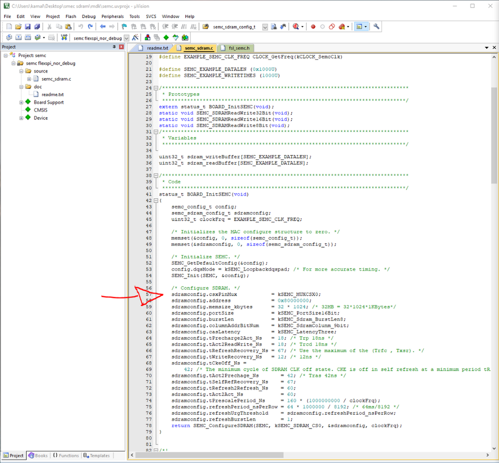
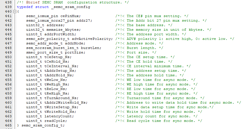
I am trying to do the same project but use the external SRAM instead of SDRAM. The SRAM base address is 0xA0000000 and has some settings that need to be set. Below, the first screenshot is the demo project with working SDRAM settings and the second screenshot is the settings needed for the SRAM.
I have tried to leave the SEMC SRAM settings as default but the program keeps failing when trying to read the data that should have been written to the SRAM. The program is successfully initialized SRAM (not sure if it is initializing in the right way) and then fails when trying to read data. The only helpful information I found is this NXP thread of someone using the same board with SEMC SRAM. I tried to use the same settings they set for their SRAM but still no success.
https://community.nxp.com/thread/480912
My main question is where can I find the correct settings to set up the SEMC with SRAM (shown in the second screenshot) and how can I map I/O into the SRAM memory space? Any information on the SEMC with SRAM is appreciated. Thanks.
SDRAM SEMC Settings:
SRAM SEMC Settings:
- Mark as New
- Bookmark
- Subscribe
- Mute
- Subscribe to RSS Feed
- Permalink
- Report Inappropriate Content
Hi,
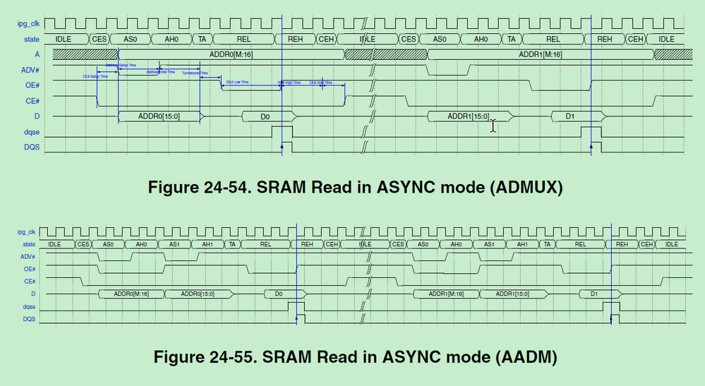
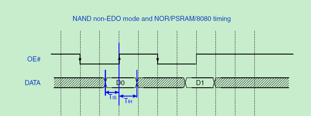
Please check below timing when SEMC SRAM mode:
What's the Enable status?
If low voltage is latch enable, from SRAM read timing, if #OE is low voltage, whatever A16 voltage level, the D1 status will be latched. It need to make sure D1 signal doesn't change voltage level at latch sampling phase.
What's the latch1 sampling time? If at #OE falling edge, that could cause problem.
From RT1050 datasheet, The sampling time should at rising edge.
Please check the Latch logic to meet the SEMC SRAM timing.
Wish it helps.
best regards,
Mike
- Mark as New
- Bookmark
- Subscribe
- Mute
- Subscribe to RSS Feed
- Permalink
- Report Inappropriate Content
The enable status must be low for the latch to activate, therefore I need OE# and A16 to be low to enable the latch.
Once the enable is low, it needs 1.5 nanoseconds to latch the data lines. The best way to find out if this latch will work with timing is to try it. I just can't figure how to set the SEMC SRAM signals.
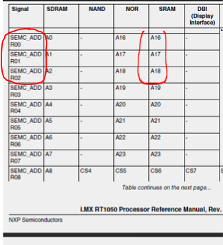
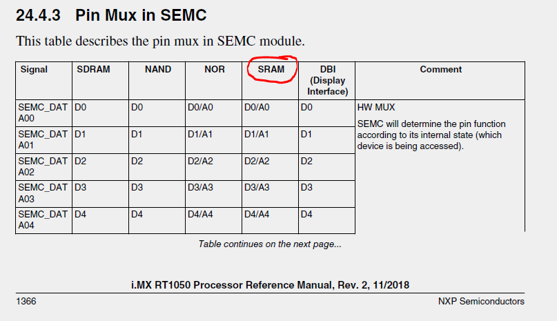
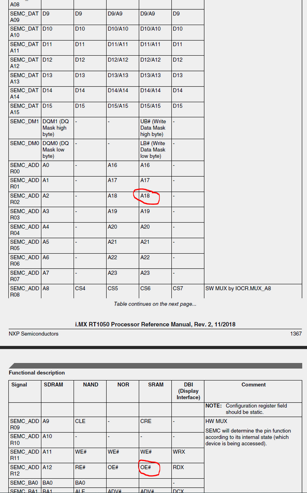
According to the SEMC Pin Mux when SRAM is initialized:
SEMC_ADDR[0] = A16
SEMC_ADDR[1] = A17
SEMC_ADDR[2] = A18
SEMC_ADDR[12] = OE#
In code, how can I set SEMC_ADDR[0] and SEMC_ADDR[12] low and SEMC_ADDR[1] and SEMC_ADDR[2] high?
- Mark as New
- Bookmark
- Subscribe
- Mute
- Subscribe to RSS Feed
- Permalink
- Report Inappropriate Content
I have figured out how to control the pins and now I am trying to invert the output signal of a pin to use for my enable.
Is there a way to inverse the an output pin signal?
I have the signal, SEMC_ADD[12] (OE#), showing high when I read in the memory location from the SRAM region. One my production board, I am using this signal as an enable that should be read low when reading from the SRAM.
I want the signal SEMC_ADD[12] (OE#) which is on pin gpio_emc_20 to be flipped so that when it outputs a low it outputs a high.
Is there anyway to flip the output signal of this pin in code instead of adding an inverter?
- Mark as New
- Bookmark
- Subscribe
- Mute
- Subscribe to RSS Feed
- Permalink
- Report Inappropriate Content
Hi Kamal,
I don't think the SEMC module software code can inverse the output pin SEMC_ADD[12] (#OE) signal.
It requires an external inverter.
best regards,
Mike
- Mark as New
- Bookmark
- Subscribe
- Mute
- Subscribe to RSS Feed
- Permalink
- Report Inappropriate Content
I am still attempting to get the latches memory mapped through SEMC SRAM, I am stuck on the the OE# signal. Everytime I read, the OE# signal goes high, and when I am not reading the signal is low. This is opposite of what should be happening as you confirmed. I even tried putting the OE# signal through an inverter and its still high when reading?
- Mark as New
- Bookmark
- Subscribe
- Mute
- Subscribe to RSS Feed
- Permalink
- Report Inappropriate Content
Hi,
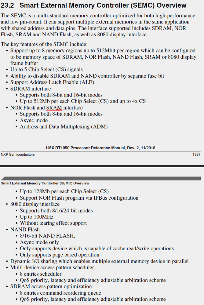
The SEMC feature shows it only support SRAM with Async mode:
There doesn't provide synchronize clock signal from SEMC module. Thanks.
best regards,
Mike
- Mark as New
- Bookmark
- Subscribe
- Mute
- Subscribe to RSS Feed
- Permalink
- Report Inappropriate Content
Hi Mike,
I finally got my SEMC with SRAM to work for my application. I was missing a critical step which was setting the pin D7 gpio for SEMC_CSX01.
Although it is working now, I am still not sure of the address mapping involved with SEMC SRAM. Currently, I am using the address lines A16, A17, and A18 as enables for my external latches. I thought that I could use address mapping to set A16, A17, and A18 low or high depending on what I want. For example, if I want to set A18 as high while leaving all the other address line signals low, I would access 0xA0040000. Likewise for A17, 0xA0020000, and A16, 0xA0010000.
This method is not working. I believe it has to do with the address mapping. Currently, I have found that accessing these addresses will fire off the corresponding address bits:
//#define BUTTON (*(volatile unsigned short *)(0xA0000000)) //A0/16, A1/17, and A2/18 low
//#define BUTTON (*(volatile unsigned short *)(0xA00C7100)) //A0/16 high and A1/17, A2/18 low
//#define BUTTON (*(volatile unsigned short *)(0xA004FA00)) //A1/17 high and A0/16, A2/18 low
//#define BUTTON (*(volatile unsigned short *)(0xA009F400)) //A2/18 high and A0/16, A1/17 low
//#define BUTTON (*(volatile unsigned short *)(0xA0116B00)) //A0/16, A1/17 high and A2/18 low
//#define BUTTON (*(volatile unsigned short *)(0xA0166500)) //A0/16, A2/18 high and A1/17 low
//#define BUTTON (*(volatile unsigned short *)(0xA00EEE00)) //A1/17, A2/18 high and A0/16 low
//#define BUTTON (*(volatile unsigned short *)(0xA01B5F00)) //A0/16, A1/17, and A2/18 high
I thought it should be like so:
//#define BUTTON (*(volatile unsigned short *)(0xA0000000)) //A0/16, A1/17, and A2/18 low
//#define BUTTON (*(volatile unsigned short *)(0xA0010000)) //A0/16 high and A1/17, A2/18 low
//#define BUTTON (*(volatile unsigned short *)(0xA0020000)) //A1/17 high and A0/16, A2/18 low
//#define BUTTON (*(volatile unsigned short *)(0xA0040000)) //A2/18 high and A0/16, A1/17 low
//#define BUTTON (*(volatile unsigned short *)(0xA0030000)) //A0/16, A1/17 high and A2/18 low
//#define BUTTON (*(volatile unsigned short *)(0xA0050000)) //A0/16, A2/18 high and A1/17 low
//#define BUTTON (*(volatile unsigned short *)(0xA0060000)) //A1/17, A2/18 high and A0/16 low
//#define BUTTON (*(volatile unsigned short *)(0xA0070000)) //A0/16, A1/17, and A2/18 high
How is address mapping configured in the SEMC SRAM? Is there an option to make it linear so that it directly corresponds with the address bits?
- Mark as New
- Bookmark
- Subscribe
- Mute
- Subscribe to RSS Feed
- Permalink
- Report Inappropriate Content
Hi,
Thanks for the info.
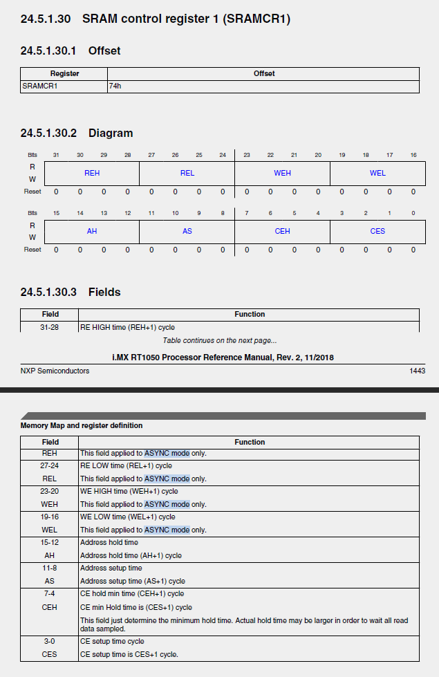
Please help to provide SEMC SRAM control register [0~3] values.
Please check the SRAM control register 0 (SRAMCR0) [AM] bits should be 0b1x (non-MUX mode) and [BL] bits be 0b000.
Wish it helps.
best regards,
Mike
- Mark as New
- Bookmark
- Subscribe
- Mute
- Subscribe to RSS Feed
- Permalink
- Report Inappropriate Content
Hi,
You mentioned SEMC SRAM signals like CS6, A18, or OE# are all output direction.
So, you can use those pins as SEMC SRAM interface pins.
Wish it helps.
best regards,
Mike
- Mark as New
- Bookmark
- Subscribe
- Mute
- Subscribe to RSS Feed
- Permalink
- Report Inappropriate Content
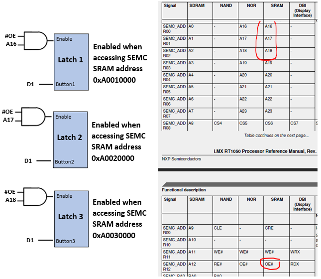
I need help setting up memory mapped I/O. How do I assign my three latches to specific memory ranges? I will be using the SEMC SRAM triggers to activate which latch I want to enable then read the desired I/O port. How do I configure my program so that if I access 0xA0010000, the signals CS6, A18, and OE# are enabled?
My current test board is using CS6, A18, and OE# as enables for my latches which are connected to my other hardware as I/O ports. My plan is to have 3 latches and use the SRAM signals to enable the desired latch through memory mapping. For example, latch one will activate when accessing 0xA0010000, latch two will activate when accessing 0xA0020000, and latch three will activate when accessing 0xA0030000. Then I will select the desired bit on the latch to read the value from.
- Mark as New
- Bookmark
- Subscribe
- Mute
- Subscribe to RSS Feed
- Permalink
- Report Inappropriate Content
Hi,
Customer could refer SEMC SDRAM demo and try to Initialize SEMC for SRAM.
Customer could call SEMC_ConfigureSRAM() SDK driver to config SEMC for SRAM.
After SEMC configured for SRAM, when access SRAM related address range, related pins will be drive.
Wish it helps.
best regards,
Mike
- Mark as New
- Bookmark
- Subscribe
- Mute
- Subscribe to RSS Feed
- Permalink
- Report Inappropriate Content
Hi Mike,
I understand that I need to configure the SRAM using SEMC_ConfigureSRAM() SDK driver, which I have already done. My issue is with memory mapping.
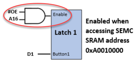
I want to use 0xA0010000 for to enable latch1 by setting SEMC_ADDR[0] low with SEMC_ADDR[1] and SEMC_ADDR[2] set as high. Therefore, when I call "0xA0010000 & bit1" I will be able to read in only bit1 from latch1 while latch2 and latch3 are disabled.
I don't know how to do this in code, not sure what syntax is used for this type of memory mapping.
For a better understanding, I attached a picture of what I am trying to complete. How can I do this in code?
Thanks again,
Kamal
- Mark as New
- Bookmark
- Subscribe
- Mute
- Subscribe to RSS Feed
- Permalink
- Report Inappropriate Content
I do not have a physical SRAM to read and write to. I just want to use the SEMC SRAM signals. I want to use signals A16, A17, A18, and OE# as enables to my latches. My question is, how do I map address 0xA0010000 to Latch1? So that when I access 0xA0010000, A16 and OE# will go low with A17 and A18 go high?
According to the SEMC Pin Mux when SRAM is initialized:
SEMC_ADDR[0] = A16
SEMC_ADDR[1] = A17
SEMC_ADDR[2] = A18
SEMC_ADDR[12] = OE#
In code, how can I set SEMC_ADDR[0] and SEMC_ADDR[12] low and SEMC_ADDR[1] and SEMC_ADDR[2] high?
I want to be able to do this in code:
if (0xA0010000 & bit1)
{ button1 is pressed }
Button1 accessed through Latch, bit1, which is only enabled when A18 and OE# are low as shown in the attachment. I have successfully initialized SEMC with SRAm, I just don't know how to map 0xA0010000 to Latch1.
- Mark as New
- Bookmark
- Subscribe
- Mute
- Subscribe to RSS Feed
- Permalink
- Report Inappropriate Content
Hi Mike,
I believe there is not a seperate part number for the SRAM. I thought it was a region of the SDRAM chip which can be used as SRAM? I am just trying to set up the SEMC with SRAM at 0xA0000000. I am a confused on if this is possible or how it is done. Here are some screenshots of the MIMXRT1050 manual showing that the SEMC can be configured with SRAM but it does not explain how. Any help or information on this subject is appreciated.
Thanks,
Kamal
- Mark as New
- Bookmark
- Subscribe
- Mute
- Subscribe to RSS Feed
- Permalink
- Report Inappropriate Content
Hi Kamal,
RT1050 reference manual SEMC module mentioned "SRAM" is another type memory device, such as MRAM or PSRAM.
I could use MR2A16ACYS35 as an example.
The MRAM device using the different hardware connection with SEMC, compared with SDRAM memory.
The SEMC using address and data multiplex mode, the low 16-bit address share the same pin with 16-bit data.
There required external address latch chip with external SRAM connection.
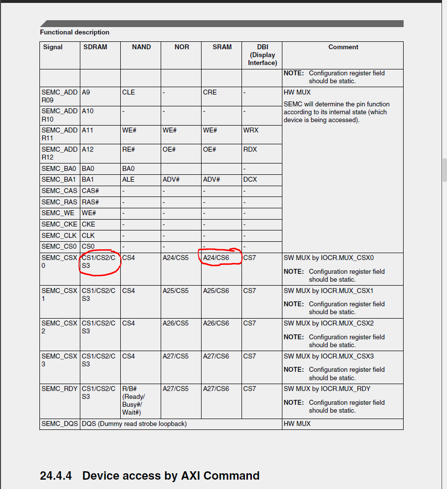
The memory range 0xA0000000 is opened to external SRAM device, which could be get from below table:
Wish it helps.
best regards,
Mike
- Mark as New
- Bookmark
- Subscribe
- Mute
- Subscribe to RSS Feed
- Permalink
- Report Inappropriate Content
Hi Mike,
So your saying that the SEMC can support SRAM at 0xA0000000 but there is none on the board. I have to add external SRAM then configure it with SEMC, correct?
If I currently do not have external SRAM and have some hardware connected to latches controlled by the SRAM Pinmux pin such as CS6, can I just set the SEMC configured with SDRAM at 0xA0000000 and using the corresponding SDRAM pin to enable the latch?
Is it possible to use the SEMC SRAM region (0xA0000000) as I/O pins instead of memory? This way I can have 3 latches and pick from them using a memory range. I am using the SEMC as if I have an external SRAM but I don't, I just want to use that memory range for my latches.
To reword the question using the screenshot, can I use CS1/CS2/CS3 (SDRAM) instead of A24/CS6 (SRAM) to enable my latch? Also, is it possible to manually set the gpio_emc_xx pins as high or low? Right now my hardware is connected to latched which are enabled using CS6 from the SEMC SRAM so I want to use the SDRAM instead.
- Mark as New
- Bookmark
- Subscribe
- Mute
- Subscribe to RSS Feed
- Permalink
- Report Inappropriate Content
Hi,
So your saying that the SEMC can support SRAM at 0xA0000000 but there is none on the board. I have to add external SRAM then configure it with SEMC, correct?
Mike: Yes, your understanding is correct.
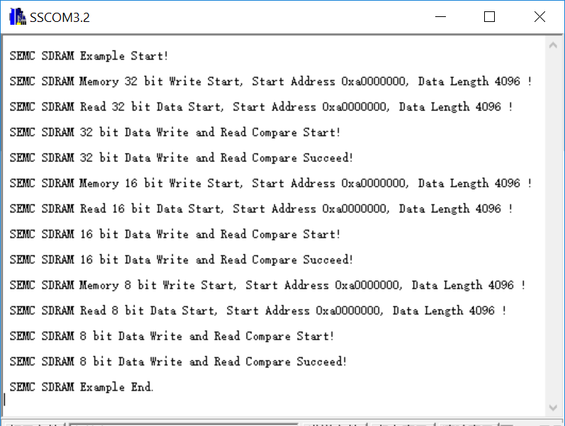
I did a test to config IMXRT1050-EVKB on board SDRAM memory at 0xA0000000, which works.
I use SDK software package provided [semc] demo, just change below codes at <semc_sdram.c>file:
Line 18 #define EXAMPLE_SEMC_START_ADDRESS (0xA0000000U)//(0x80000000U)
Line 58 sdramconfig.address = 0xA0000000;//0x80000000;
After that, the SDRAM could be access with start address at 0xA0000000.
About SDRAM related pins latch, I think it works.
best regards,
Mike
- Mark as New
- Bookmark
- Subscribe
- Mute
- Subscribe to RSS Feed
- Permalink
- Report Inappropriate Content
Hi Mike,
Thanks for all the responses, I understand much better now. I also already tried the SDRAM example at 0xA0000000 and it was successful like yours.
My last question is, since I don't have an SRAM, I cannot configure the SEMC with SRAM. Therefore, does that mean I will not be able to use any of the SEMC SRAM signals like CS6, A18, or OE#?
My current test board is using CS6, A18, and OE# as enables for my latches which are connected to my other hardware as I/O ports. My plan was to have 3 latches and use the SRAM signals to enable the desired latch through memory mapping. For example, latch one will activate when accessing 0xA0010000, latch two will activate when accessing 0xA0020000, and latch three will activate when accessing 0xA0030000. Then I will select the desired bit on the latch to read the value from.
Will I need to change the signals to match the SDRAM instead or can I use the corresponding signals from the SDRAM?
For example, instead of using the CS6 signal for SEMC_CSX0, can I use the SDRAM signal CS1/CS2/CS3?
Thanks,
Kamal
- Mark as New
- Bookmark
- Subscribe
- Mute
- Subscribe to RSS Feed
- Permalink
- Report Inappropriate Content
Sorry for the confusion, let me reword my question.
I want to use the SRAM region of the SEMC from the MIMXRT1050 demo board as I/O ports. I will have three Latch chips, https://datasheet.ciiva.com/4829/74lcx16373-101227-4829686.pdf , where the enables will be the SRAM chip selects. For example, if I have button1 on Latch chip1 will be accessed through SRAM chip select 1 and button2 on Latch chip2 will be accessed through SRAM chip select 2.
My questions are:
1. Can I use the SRAM region of the SEMC from the MIMXRT1050 demo board to get values from I/O ports?
2. Where and how do I configure the SRAM region of the SEMC?
3. I want to be able to access a specific memory region and have SEMC know which chip enables to trigger (memory mapping), will I need to define the memory regions to the chip selects?
4. I will be using the SEMC with SRAM and external SDRAM at the same time, will I need to keep manually switching between the different regions or will SEMC do it automatically depending on the address range?
- Mark as New
- Bookmark
- Subscribe
- Mute
- Subscribe to RSS Feed
- Permalink
- Report Inappropriate Content
kamal1,
The thread ended without resolution and I am curious if you ultimately succeeded or found support insufficient and moved on.
I am similarly desiring to memory map a device, a LON5000, that presently is memory mapped onto a MCF5206E ColdFire CPU, the CPU having gone EOL. Like your latches it is otherwise simple - 8 data, 1 address, WE# and CE#. I should be a piece of cake to memory map as it was in its day, as would be your latches.
For others reading, SEMC is already hosting SDRAM and NAND. The CPU is the 1175. FLEXIO1 and 2 were mercilessly destroyed by MCUExpresso along with much else - the chip needs far more pins than as packaged. With the 117x the tool becomes PTSDExpresso.
I'd start a new thread, but our needs are the same. You went quiet and perhaps you succeeded. One can hope. I'm reluctant to spin a PCB if you couldn't ultimately resolve, i.e. there appear to be no functional solutions posted yet, and NXP dismissively states "Use FLEXIO". Yes, if there were 100 more pins on the 1175 it might have worked. Thank you.
Best Regards, Ed
