- NXP Forums
- Product Forums
- General Purpose MicrocontrollersGeneral Purpose Microcontrollers
- i.MX Forumsi.MX Forums
- QorIQ Processing PlatformsQorIQ Processing Platforms
- Identification and SecurityIdentification and Security
- Power ManagementPower Management
- MCX Microcontrollers
- S32G
- S32K
- S32V
- MPC5xxx
- Other NXP Products
- Wireless Connectivity
- S12 / MagniV Microcontrollers
- Powertrain and Electrification Analog Drivers
- Sensors
- Vybrid Processors
- Digital Signal Controllers
- 8-bit Microcontrollers
- ColdFire/68K Microcontrollers and Processors
- PowerQUICC Processors
- OSBDM and TBDML
-
- Solution Forums
- Software Forums
- MCUXpresso Software and ToolsMCUXpresso Software and Tools
- CodeWarriorCodeWarrior
- MQX Software SolutionsMQX Software Solutions
- Model-Based Design Toolbox (MBDT)Model-Based Design Toolbox (MBDT)
- FreeMASTER
- eIQ Machine Learning Software
- Embedded Software and Tools Clinic
- S32 SDK
- S32 Design Studio
- Vigiles
- GUI Guider
- Zephyr Project
- Voice Technology
- Application Software Packs
- Secure Provisioning SDK (SPSDK)
- Processor Expert Software
-
- Topics
- Mobile Robotics - Drones and RoversMobile Robotics - Drones and Rovers
- NXP Training ContentNXP Training Content
- University ProgramsUniversity Programs
- Rapid IoT
- NXP Designs
- SafeAssure-Community
- OSS Security & Maintenance
- Using Our Community
-
-
- Home
- :
- i.MX Forums
- :
- i.MX RT Knowledge Base
- :
- How to enable DDR mode
How to enable DDR mode
- Subscribe to RSS Feed
- Mark as New
- Mark as Read
- Bookmark
- Subscribe
- Printer Friendly Page
- Report Inappropriate Content
How to enable DDR mode
How to enable DDR mode
As we know, the RT series MCUs support the XIP (Execute in place) mode and benefit from saving the number of pins, serial NOR Flash is most commonly used, as the FlexSPI module can high efficient fetch the code and data from the Serial NOR flash for Cortex-M7 to execute.
The fetch way is implementing via utilizing the Quad IO Fast Read command, meanwhile, the serail NOR flash works in the SDR (Single Data transfer Rate) mode, it receives data on SCLK rise edge and transmits data on SCLK fall edge. Comparing to the SDR mode, the DDR (Dual Data transfer Rate) mode has a higher throughput capacity, whether it can provide better performance of XIP mode, and how to do that if we want the Serial NOR Flash to work in DDR (Dual Data transfer Rate) mode?
SDR & DDR mode
SDR mode:
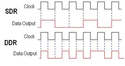
In SDR (Single Data transfer Rate) mode, data is only clocked on one edge of the clock (either the rising or falling edge). This means that for SDR to have data being transmitted at X Mbps, the clock bit rate needs to be 2X Mbps.
DDR mode:
For DDR (Dual Data transfer Rate) mode, also known as DTR (Dual Transfer Rate) mode, data is transferred on both the rising and falling edge of the clock. This means data is transmitted at X Mbps only requires the clock bit rate to be X Mbps, hence doubling the bandwidth (as Fig 1 shows).
Fig 1
Enable DDR mode
The below steps illustrate how to make the i.MX RT1060 boot from the QSPI with working in DDR mode.
Note: The board is MIMXRT1060, IDE is MCUXpresso IDE
-
Open a hello_world as the template
-
Modify the FDCB(Flash Device Configuration Block)
a)Set the controllerMiscOption parameter to supports DDR read command.
b) Set Serial Flash frequency to 60 MHz.
c)Parase the DDR read command into command sequence.
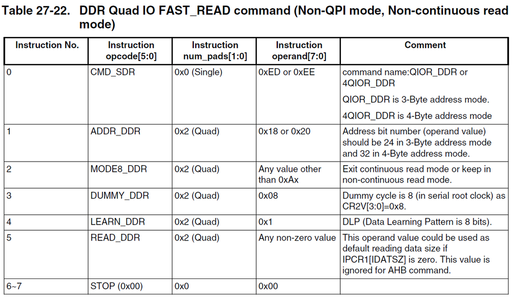
The following table shows a template command sequence of DDR Quad IO FAST READ instruction and it's almost matching with the FRQDTR (Fast Read Quad IO DTR) Sequence of IS25WP064 (as Fig 2 shows).Fig2 FRQDTR Sequence
d)Adjust the dummy cycles.
The dummy cycles should match with the specific serial clock frequency and the default dummy cycles of the FRQDTR sequence command is 6 (as the below table shows).
However, when the serial clock frequency is 60MHz, the dummy cycle should change to 4 (as the below table shows).
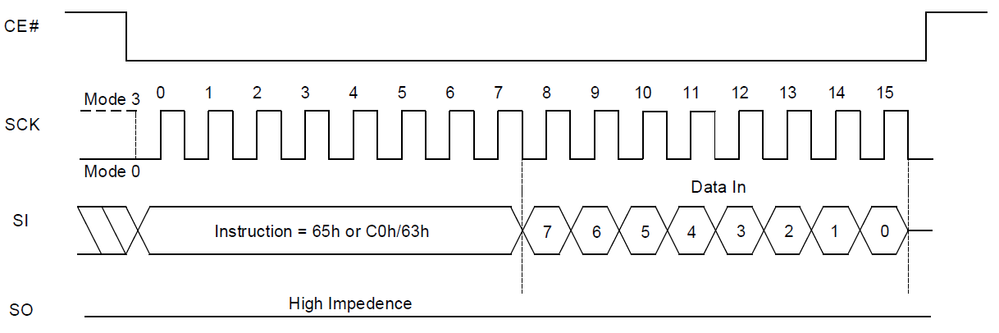
So it needs to configure [P6:P3] bits of the Read Register (as the below table shows) via adding the SET READ PARAMETERS command sequence(as Fig 3 shows) in FDCB manually.
Fig 3 SET READ PARAMETERS command sequence
In further, in DDR mode, the SCLK cycle is double the serial root clock cycle. The operand value should be set as 2N, 2N-1 or 2*N+1 depending on how the dummy cycles defined in the device datasheet.
In the end, we can get an adjusted FCDB like below.
// Set Dummy Cycles
#define FLASH_DUMMY_CYCLES      8
// Set Read register command sequence's Index in LUT table
#define CMD_LUT_SEQ_IDX_SET_READ_PARAM 7
// Read,Read Status,Write Enable command sequences' Index in LUT table
#define CMD_LUT_SEQ_IDX_READ           0
#define CMD_LUT_SEQ_IDX_READSTATUS     1
#define CMD_LUT_SEQ_IDX_WRITEENABLE    3

const flexspi_nor_config_t qspiflash_config = {
    .memConfig =
        {
            .tag              = FLEXSPI_CFG_BLK_TAG,
            .version          = FLEXSPI_CFG_BLK_VERSION,
            .readSampleClksrc=kFlexSPIReadSampleClk_LoopbackFromDqsPad,
            .csHoldTime       = 3u,
            .csSetupTime      = 3u,
            // Enable DDR mode
            .controllerMiscOption = kFlexSpiMiscOffset_DdrModeEnable | kFlexSpiMiscOffset_SafeConfigFreqEnable,

            .sflashPadType    = kSerialFlash_4Pads,
            //.serialClkFreq    = kFlexSpiSerialClk_100MHz,
   .serialClkFreq    = kFlexSpiSerialClk_60MHz,
            .sflashA1Size     = 8u * 1024u * 1024u,

            // Enable Flash register configuration
            .configCmdEnable = 1u,
            .configModeType[0] = kDeviceConfigCmdType_Generic,
            .configCmdSeqs[0] =
                {
                    .seqNum = 1,
                    .seqId = CMD_LUT_SEQ_IDX_SET_READ_PARAM,
                    .reserved = 0,
                },

            .lookupTable =
                {
            // Read LUTs
     [4*CMD_LUT_SEQ_IDX_READ]     = FLEXSPI_LUT_SEQ(CMD_SDR,   FLEXSPI_1PAD, 0xED, RADDR_DDR, FLEXSPI_4PAD, 0x18),
     // The MODE8_DDR subsequence costs 2 cycles that is part of the whole dummy cycles
     [4*CMD_LUT_SEQ_IDX_READ + 1] = FLEXSPI_LUT_SEQ(MODE8_DDR, FLEXSPI_4PAD, 0x00, DUMMY_DDR, FLEXSPI_4PAD, FLASH_DUMMY_CYCLES-2),
     [4*CMD_LUT_SEQ_IDX_READ + 2] = FLEXSPI_LUT_SEQ(READ_DDR,  FLEXSPI_4PAD, 0x04, STOP,      FLEXSPI_1PAD, 0x00),

     // READ STATUS REGISTER
     [4*CMD_LUT_SEQ_IDX_READSTATUS]   = FLEXSPI_LUT_SEQ(CMD_SDR, FLEXSPI_1PAD, 0x05, READ_SDR,  FLEXSPI_1PAD, 0x01),
     [4*CMD_LUT_SEQ_IDX_READSTATUS + 1] = FLEXSPI_LUT_SEQ(STOP, FLEXSPI_1PAD, 0x00, 0, 0, 0),
      // WRTIE ENABLE
     [4*CMD_LUT_SEQ_IDX_WRITEENABLE] = FLEXSPI_LUT_SEQ(CMD_SDR,FLEXSPI_1PAD, 0x06, STOP, FLEXSPI_1PAD, 0x00),

      // Set Read register
     [4*CMD_LUT_SEQ_IDX_SET_READ_PARAM]      = FLEXSPI_LUT_SEQ(CMD_SDR,FLEXSPI_1PAD, 0x63, WRITE_SDR, FLEXSPI_1PAD, 0x01),
     [4*CMD_LUT_SEQ_IDX_SET_READ_PARAM + 1] = FLEXSPI_LUT_SEQ(STOP,FLEXSPI_1PAD, 0x00, 0, 0, 0),

                },
        },
    .pageSize           = 256u,
    .sectorSize         = 4u * 1024u,
    .blockSize          = 64u * 1024u,
    .isUniformBlockSize = false,
};
Is DDR mode real better?
According to the RT1060's datasheet, the below table illustrates the maximum frequency of FlexSPI operation, as the MIMXRT1060's onboard QSPI flash is IS25WP064AJBLE, it doesn't contain the MQS pin, it means set MCR0.RXCLKsrc=1 (Internal dummy read strobe and loopbacked from DQS) is the most optimized option.
operation mode RXCLKsrc=0 RXCLKsrc=1 RXCLKsrc=3 SDR 60 MHz 133 MHz 166 MHz DDR 30 MHz 66 MHz 166 MHz In another word, QSPI can run up to 133 MHz in SDR mode versus 66 MHz in DDR mode. From the perspective of throughput capacity, they're almost the same. It seems like DDR mode is not a better option for IS25WP064AJBLE and the following experiment will validate the assumption.
Experiment
-
mbedtls_benchmark
I use the mbedtls_benchmark as the first testing demo and I run the demo under the below conditions:
-
100MH, SDR mode; -
133MHz, SDR mode; -
66MHz, DDR mode;
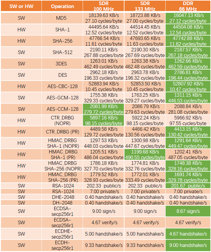
According to the corresponding printout information (as below shows), I make a table for comparison and I mark the worst performance of implementation items among the above three conditions, just as Fig 4 shows.
SDR Mode run at 100 MHz.
FlexSPI clock source is 3, FlexSPI Div is 6, PllPfd2Clk is 720000000
mbedTLS version 2.16.6
fsys=600000000
Using following implementations:
  SHA: DCP HW accelerated
  AES: DCP HW accelerated
  AES GCM: Software implementation
  DES: Software implementation
  Asymmetric cryptography: Software implementation

  MD5                      :  18139.63 KB/s,   27.10 cycles/byte
  SHA-1                    :  44495.64 KB/s,   12.52 cycles/byte
  SHA-256                  :  47766.54 KB/s,   11.61 cycles/byte
  SHA-512                  :  2190.11 KB/s,  267.88 cycles/byte
  3DES                     :  1263.01 KB/s,  462.49 cycles/byte
  DES                      :  2962.18 KB/s,  196.33 cycles/byte
  AES-CBC-128              :  52883.94 KB/s,   10.45 cycles/byte
  AES-GCM-128              :  1755.38 KB/s,  329.33 cycles/byte
  AES-CCM-128              :  2081.99 KB/s,  279.72 cycles/byte
  CTR_DRBG (NOPR)          :  5897.16 KB/s,   98.15 cycles/byte
  CTR_DRBG (PR)            :  4489.58 KB/s,  129.72 cycles/byte
  HMAC_DRBG SHA-1 (NOPR)   :  1297.53 KB/s,  448.03 cycles/byte
  HMAC_DRBG SHA-1 (PR)     :  1205.51 KB/s,  486.04 cycles/byte
  HMAC_DRBG SHA-256 (NOPR) :  1786.18 KB/s,  327.70 cycles/byte
  HMAC_DRBG SHA-256 (PR)   :  1779.52 KB/s,  328.93 cycles/byte
  RSA-1024                 :  202.33  public/s
  RSA-1024                 :    7.00 private/s
  DHE-2048                 :    0.40 handshake/s
  DH-2048                  :    0.40 handshake/s
  ECDSA-secp256r1          :    9.00 sign/s
  ECDSA-secp256r1          :    4.67 verify/s
  ECDHE-secp256r1          :    5.00 handshake/s
  ECDH-secp256r1           :    9.33 handshake/s
DDR Mode run at 66 MHz. FlexSPI clock source is 2, FlexSPI Div is 5, PllPfd2Clk is 396000000 mbedTLS version 2.16.6 fsys=600000000 Using following implementations: SHA: DCP HW accelerated AES: DCP HW accelerated AES GCM: Software implementation DES: Software implementation Asymmetric cryptography: Software implementation MD5 : 16047.13 KB/s, 27.12 cycles/byte SHA-1 : 44504.08 KB/s, 12.54 cycles/byte SHA-256 : 47742.88 KB/s, 11.62 cycles/byte SHA-512 : 2187.57 KB/s, 267.18 cycles/byte 3DES : 1262.66 KB/s, 462.59 cycles/byte DES : 2786.81 KB/s, 196.44 cycles/byte AES-CBC-128 : 52807.92 KB/s, 10.47 cycles/byte AES-GCM-128 : 1311.15 KB/s, 446.53 cycles/byte AES-CCM-128 : 2088.84 KB/s, 281.08 cycles/byte CTR_DRBG (NOPR) : 5966.92 KB/s, 97.55 cycles/byte CTR_DRBG (PR) : 4413.15 KB/s, 130.42 cycles/byte HMAC_DRBG SHA-1 (NOPR) : 1291.64 KB/s, 449.47 cycles/byte HMAC_DRBG SHA-1 (PR) : 1202.41 KB/s, 487.05 cycles/byte HMAC_DRBG SHA-256 (NOPR) : 1748.38 KB/s, 328.16 cycles/byte HMAC_DRBG SHA-256 (PR) : 1691.74 KB/s, 329.78 cycles/byte RSA-1024 : 201.67 public/s RSA-1024 : 7.00 private/s DHE-2048 : 0.40 handshake/s DH-2048 : 0.40 handshake/s ECDSA-secp256r1 : 8.67 sign/s ECDSA-secp256r1 : 4.67 verify/s ECDHE-secp256r1 : 4.67 handshake/s ECDH-secp256r1 : 9.00 handshake/sFig 4 Performance comparison
We can find that most of the implementation items are achieve the worst performance when QSPI works in DDR mode with 66 MHz.
-
Coremark demo
The second demo is running the Coremark demo under the above three conditions and the result is illustrated below.
SDR Mode run at 100 MHz.
FlexSPI clock source is 3, FlexSPI Div is 6, PLL3 PFD0 is 720000000

2K performance run parameters for coremark.
CoreMark Size    : 666
Total ticks      : 391889200
Total time (secs): 16.328717
Iterations/Sec   : 2449.671999
Iterations       : 40000
Compiler version : MCUXpresso IDE v11.3.1
Compiler flags   : Optimization most (-O3)
Memory location  : STACK
seedcrc          : 0xe9f5
[0]crclist       : 0xe714
[0]crcmatrix     : 0x1fd7
[0]crcstate      : 0x8e3a
[0]crcfinal      : 0x25b5
Correct operation validated. See readme.txt for run and reporting rules.
CoreMark 1.0 : 2449.671999 / MCUXpresso IDE v11.3.1 Optimization most (-O3) / STACK
SDR Mode run at 133 MHz. FlexSPI clock source is 3, FlexSPI Div is 4, PLL3 PFD0 is 664615368 2K performance run parameters for coremark. CoreMark Size : 666 Total ticks : 391888682 Total time (secs): 16.328695 Iterations/Sec : 2449.675237 Iterations : 40000 Compiler version : MCUXpresso IDE v11.3.1 Compiler flags : Optimization most (-O3) Memory location : STACK seedcrc : 0xe9f5 [0]crclist : 0xe714 [0]crcmatrix : 0x1fd7 [0]crcstate : 0x8e3a [0]crcfinal : 0x25b5 Correct operation validated. See readme.txt for run and reporting rules. CoreMark 1.0 : 2449.675237 / MCUXpresso IDE v11.3.1 Optimization most (-O3) / STACKDDR Mode run at 66 MHz. FlexSPI clock source is 2, FlexSPI Div is 5, PLL3 PFD0 is 396000000 2K performance run parameters for coremark. CoreMark Size : 666 Total ticks : 391890772 Total time (secs): 16.328782 Iterations/Sec : 2449.662173 Iterations : 40000 Compiler version : MCUXpresso IDE v11.3.1 Compiler flags : Optimization most (-O3) Memory location : STACK seedcrc : 0xe9f5 [0]crclist : 0xe714 [0]crcmatrix : 0x1fd7 [0]crcstate : 0x8e3a [0]crcfinal : 0x25b5 Correct operation validated. See readme.txt for run and reporting rules. CoreMark 1.0 : 2449.662173 / MCUXpresso IDE v11.3.1 Optimization most (-O3) / STACKAfter comparing the CoreMark scores, it gets the lowest CoreMark score when QSPI works in DDR mode with 66 MHz. However, they're actually pretty close.
Through the above two testings, we can get the DDR mode maybe not a better option, at least for the i.MX RT10xx series MCU.
-


