
- Forums
- Product Forums
- General Purpose MicrocontrollersGeneral Purpose Microcontrollers
- i.MX Forumsi.MX Forums
- QorIQ Processing PlatformsQorIQ Processing Platforms
- Identification and SecurityIdentification and Security
- Power ManagementPower Management
- Wireless ConnectivityWireless Connectivity
- RFID / NFCRFID / NFC
- Advanced AnalogAdvanced Analog
- Neural Processing UnitsNeural Processing Units
- MCX Microcontrollers
- S32G
- S32K
- S32V
- MPC5xxx
- Other NXP Products
- S12 / MagniV Microcontrollers
- Powertrain and Electrification Analog Drivers
- Sensors
- Vybrid Processors
- Digital Signal Controllers
- 8-bit Microcontrollers
- ColdFire/68K Microcontrollers and Processors
- PowerQUICC Processors
- OSBDM and TBDML
- S32M
- S32Z/E
-
- Solution Forums
- Software Forums
- MCUXpresso Software and ToolsMCUXpresso Software and Tools
- CodeWarriorCodeWarrior
- MQX Software SolutionsMQX Software Solutions
- Model-Based Design Toolbox (MBDT)Model-Based Design Toolbox (MBDT)
- FreeMASTER
- eIQ Machine Learning Software
- Embedded Software and Tools Clinic
- S32 SDK
- S32 Design Studio
- GUI Guider
- Zephyr Project
- Voice Technology
- Application Software Packs
- Secure Provisioning SDK (SPSDK)
- Processor Expert Software
- Generative AI & LLMs
-
- Topics
- Mobile Robotics - Drones and RoversMobile Robotics - Drones and Rovers
- NXP Training ContentNXP Training Content
- University ProgramsUniversity Programs
- Rapid IoT
- NXP Designs
- SafeAssure-Community
- OSS Security & Maintenance
- Using Our Community
-
- Cloud Lab Forums
-
- Knowledge Bases
- ARM Microcontrollers
- i.MX Processors
- Identification and Security
- Model-Based Design Toolbox (MBDT)
- QorIQ Processing Platforms
- S32 Automotive Processing Platform
- Wireless Connectivity
- CodeWarrior
- MCUXpresso Suite of Software and Tools
- MQX Software Solutions
- RFID / NFC
- Advanced Analog
- Neural Processing Units
-
- NXP Tech Blogs
- Home
- :
- i.MX フォーラム
- :
- i.MXグラフィックス
- :
- Re: i.MX8QXP Display Controller Pixel Link to LCDIF Configuration
i.MX8QXP Display Controller Pixel Link to LCDIF Configuration
- RSS フィードを購読する
- トピックを新着としてマーク
- トピックを既読としてマーク
- このトピックを現在のユーザーにフロートします
- ブックマーク
- 購読
- ミュート
- 印刷用ページ
- 新着としてマーク
- ブックマーク
- 購読
- ミュート
- RSS フィードを購読する
- ハイライト
- 印刷
- 不適切なコンテンツを報告
Hello,
Im trying to connect the display controller output to the eLCDIF interface in the ADMA subsystem.
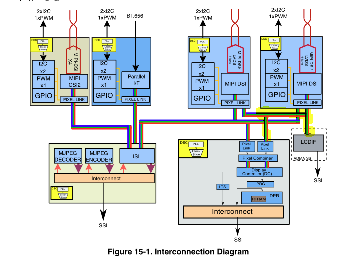
The block diagram in section 15.1.1.1 of the reference manual shows a possible connection using the pixel link, but provides no further information.
I have looked at the SDK examples for the i.MX8 but there are noone provided for the eLCDIF interface.
Furthermore the SDK examples for the DPU also dont show how outputting to the eLCDIF interface would be done, only how to select one of the two lvds channels.
How could I set about to acomplish this? As far as I can tell the so called "pixel link" is a AXI bus, which means there should be a axi master (LCDIF) which I would have to connect with an axi slave (the pixel link of the dc?).
Thanks in advance.
解決済! 解決策の投稿を見る。
- 新着としてマーク
- ブックマーク
- 購読
- ミュート
- RSS フィードを購読する
- ハイライト
- 印刷
- 不適切なコンテンツを報告
I found the solution to my issue: after setting up display stream 1, setting the pixel link slave index to 1 and changing the lcdif mux bit 1:0 to 1, you still need to enable the pixel link mux clock to the pixel clock frequency. The eLCDIF module doesnt need to be configured at all.

- 新着としてマーク
- ブックマーク
- 購読
- ミュート
- RSS フィードを購読する
- ハイライト
- 印刷
- 不適切なコンテンツを報告
Could you tell us which board and which version of BSP are you using?
- 新着としてマーク
- ブックマーク
- 購読
- ミュート
- RSS フィードを購読する
- ハイライト
- 印刷
- 不適切なコンテンツを報告
Im using a custom in-house carrier board and the BSP Version SDK_2.9.0_MIMX8QX5xxxFZ.
- 新着としてマーク
- ブックマーク
- 購読
- ミュート
- RSS フィードを購読する
- ハイライト
- 印刷
- 不適切なコンテンツを報告
Pixel link is dedicated bus used for transferring pixel between master (DISPLAY ) and slave (with fix address. )
The address the master is sending to is configured though SCU FW call.
The document "sc_fw_api_qx_b0.pdf" part of the imx-scfw-porting-kit is describing the API:

That's what the following chapter is trying to explain in the RM:

But I would have expected to be find it in the RM chapter:

Verification on the errata: nothing is preventing to to configure the pixel address.
But looking at the latest internal documentation, it feels like the feature has been de-scoped
- 新着としてマーク
- ブックマーク
- 購読
- ミュート
- RSS フィードを購読する
- ハイライト
- 印刷
- 不適切なコンテンツを報告
Thanks for the answer.
I'm am still unsure on which value to write to the SC_C_PXL_LINK_MST1_ADDR resource, if I want to use the eLCDIF interface as an output.
Looking at the dpu_character SDK example, it seems like this value is always 0 for LVDS or DSI, the only difference is the DPU display index.
Do I need to take additional steps to output to the eLCDIF or is there a simple address I need to use for the SC_C_PXL_LINK_MST1_ADDR resource?
#if (DPU_EXAMPLE_DI == DPU_DI_MIPI)
status_t SOC_SetDpuMipiDsiPixelLink(sc_ipc_t ipc, IRIS_MVPL_Type *dpu, uint8_t displayIndex, MIPI_DSI_HOST_Type *dsi)
{
    /*
     * Pixel link setting.
     *
     * DPU 0 display0 is connected to MIPI DSI 0 using address 0.
     * DPU 0 display1 is connected to MIPI DSI 1 using address 0.
     *
     * SC_R_DC_0    SC_C_PXL_LINK_MST1_ADDR   Master 1 pixel link address
     * SC_R_DC_0    SC_C_PXL_LINK_MST1_ENB    Master 1 pixel link enable
     * SC_R_DC_0    SC_C_PXL_LINK_MST1_VLD    Master 1 pixel link valid
     * SC_R_DC_0    SC_C_PXL_LINK_MST2_ADDR   Master 2 pixel link address
     * SC_R_DC_0    SC_C_PXL_LINK_MST2_ENB    Master 2 pixel link enable
     * SC_R_DC_0    SC_C_PXL_LINK_MST2_VLD    Master 2 pixel link valid
     * SC_R_DC_0    SC_C_SYNC_CTRL0           PL sync ctrl 0
     * SC_R_DC_0    SC_C_SYNC_CTRL1           PL sync ctrl 1
     */
    uint8_t pixelLinkAddr = 0;
    uint32_t i;
    sc_err_t err = SC_ERR_NONE;

    const dpu_mipi_pl_addr_t dpuMipiPlAddrs[] = {
        {
            .dpu             = DC__IRIS_MVPL,
            .dpuDisplayIndex = 0,
            .dsi             = DI_MIPI_DSI_LVDS_0__MIPI_DSI_HOST,
            .plAddr          = 0,
        },
        {
            .dpu             = DC__IRIS_MVPL,
            .dpuDisplayIndex = 1,
            .dsi             = DI_MIPI_DSI_LVDS_1__MIPI_DSI_HOST,
            .plAddr          = 0,
        },
    };

    const sc_ctrl_t pixelLinkCtrl[][4] = {
        {
            SC_C_PXL_LINK_MST1_ADDR,
            SC_C_PXL_LINK_MST1_ENB,
            SC_C_PXL_LINK_MST1_VLD,
            SC_C_SYNC_CTRL0,
        },
        {
            SC_C_PXL_LINK_MST2_ADDR,
            SC_C_PXL_LINK_MST2_ENB,
            SC_C_PXL_LINK_MST2_VLD,
            SC_C_SYNC_CTRL1,
        },
    };

    /* Get the pixel link address. */
    for (i = 0; i < ARRAY_SIZE(dpuMipiPlAddrs); i++)
    {
        if ((dpu == dpuMipiPlAddrs[i].dpu) && (displayIndex == dpuMipiPlAddrs[i].dpuDisplayIndex) &&
            (dsi == dpuMipiPlAddrs[i].dsi))
        {
            pixelLinkAddr = dpuMipiPlAddrs[i].plAddr;
            break;
        }
    }

    if (ARRAY_SIZE(dpuMipiPlAddrs) <= i)
    {
        PRINTF("ERROR: This DPU to MIPI DSI path is not supported.\r\n");
        return kStatus_Fail;
    }

    /* Set address. */
    err = sc_misc_set_control(ipc, DC_RSRC, pixelLinkCtrl[displayIndex][0], pixelLinkAddr);
    if (SC_ERR_NONE != err)
    {
        assert(false);
    }

    /* Pull down sync control. */
    err = sc_misc_set_control(ipc, DC_RSRC, pixelLinkCtrl[displayIndex][3], 0);
    if (SC_ERR_NONE != err)
    {
        assert(false);
    }

    /* Enable pixel link. */
    err = sc_misc_set_control(ipc, DC_RSRC, pixelLinkCtrl[displayIndex][1], 1);
    if (SC_ERR_NONE != err)
    {
        assert(false);
    }

    /* Delay at least 3 pixel clock. */
    for (volatile uint32_t i = 0; i < 0x100000; i++)
    {
    }

    /* Valid pixel link. */
    err = sc_misc_set_control(ipc, DC_RSRC, pixelLinkCtrl[displayIndex][2], 1);
    if (SC_ERR_NONE != err)
    {
        assert(false);
    }

    /* Pull up sync control. */
    err = sc_misc_set_control(ipc, DC_RSRC, pixelLinkCtrl[displayIndex][3], 1);
    if (SC_ERR_NONE != err)
    {
        assert(false);
    }

    return kStatus_Success;
}
#elif (DPU_EXAMPLE_DI == DPU_DI_LVDS)
status_t SOC_SetDpuLdbPixelLink(sc_ipc_t ipc, IRIS_MVPL_Type *dpu, uint8_t displayIndex, LDB_Type *ldb)
{
    /*
     * Pixel link setting.
     *
     * DPU 0 display1 is connected to LDB 0 using address 0.
     * DPU 1 display1 is connected to LDB 1 using address 0.
     *
     * SC_R_DC_0    SC_C_PXL_LINK_MST1_ADDR   Master 1 pixel link address
     * SC_R_DC_0    SC_C_PXL_LINK_MST1_ENB    Master 1 pixel link enable
     * SC_R_DC_0    SC_C_PXL_LINK_MST1_VLD    Master 1 pixel link valid
     * SC_R_DC_0    SC_C_PXL_LINK_MST2_ADDR   Master 2 pixel link address
     * SC_R_DC_0    SC_C_PXL_LINK_MST2_ENB    Master 2 pixel link enable
     * SC_R_DC_0    SC_C_PXL_LINK_MST2_VLD    Master 2 pixel link valid
     * SC_R_DC_0    SC_C_SYNC_CTRL0           PL sync ctrl 0
     * SC_R_DC_0    SC_C_SYNC_CTRL1           PL sync ctrl 1
     */
    uint8_t pixelLinkAddr = 0;
    uint32_t i;
    sc_err_t err = SC_ERR_NONE;

    const dpu_ldb_pl_addr_t dpuLdbPlAddrs[] = {
        {
            .dpu             = DC__IRIS_MVPL,
            .dpuDisplayIndex = 0,
            .ldb             = MIPI_DSI_LVDS_COMBO0_CSR,
            .plAddr          = 0,
        },
        {
            .dpu             = DC__IRIS_MVPL,
            .dpuDisplayIndex = 1,
            .ldb             = MIPI_DSI_LVDS_COMBO1_CSR,
            .plAddr          = 0,
        },
    };

    const sc_ctrl_t pixelLinkCtrl[][4] = {
        {
            SC_C_PXL_LINK_MST1_ADDR,
            SC_C_PXL_LINK_MST1_ENB,
            SC_C_PXL_LINK_MST1_VLD,
            SC_C_SYNC_CTRL0,
        },
        {
            SC_C_PXL_LINK_MST2_ADDR,
            SC_C_PXL_LINK_MST2_ENB,
            SC_C_PXL_LINK_MST2_VLD,
            SC_C_SYNC_CTRL1,
        },
    };

    /* Get the pixel link address. */
    for (i = 0; i < ARRAY_SIZE(dpuLdbPlAddrs); i++)
    {
        if ((dpu == dpuLdbPlAddrs[i].dpu) && (displayIndex == dpuLdbPlAddrs[i].dpuDisplayIndex) &&
            (ldb == dpuLdbPlAddrs[i].ldb))
        {
            pixelLinkAddr = dpuLdbPlAddrs[i].plAddr;
            break;
        }
    }

    if (ARRAY_SIZE(dpuLdbPlAddrs) <= i)
    {
        PRINTF("ERROR: This DPU to LDB path is not supported.\r\n");
        return kStatus_Fail;
    }

    /* 8QX uses combo PHY, configure to LVDS here. */
    err = sc_misc_set_control(ipc, MIPI_DSI_RSRC, SC_C_MODE, 1);
    if (SC_ERR_NONE != err)
    {
        assert(false);
    }

    err = sc_misc_set_control(ipc, MIPI_DSI_RSRC, SC_C_DUAL_MODE, 0);
    if (SC_ERR_NONE != err)
    {
        assert(false);
    }

    err = sc_misc_set_control(ipc, MIPI_DSI_RSRC, SC_C_PXL_LINK_SEL, 0);
    if (SC_ERR_NONE != err)
    {
        assert(false);
    }

    /* Set address. */
    err = sc_misc_set_control(ipc, DC_RSRC, pixelLinkCtrl[displayIndex][0], pixelLinkAddr);
    if (SC_ERR_NONE != err)
    {
        assert(false);
    }

    /* Pull down sync control. */
    err = sc_misc_set_control(ipc, DC_RSRC, pixelLinkCtrl[displayIndex][3], 0);
    if (SC_ERR_NONE != err)
    {
        assert(false);
    }

    /* Enable pixel link. */
    err = sc_misc_set_control(ipc, DC_RSRC, pixelLinkCtrl[displayIndex][1], 1);
    if (SC_ERR_NONE != err)
    {
        assert(false);
    }

    /* Delay at least 3 pixel clock. */
    for (volatile uint32_t i = 0; i < 0x100000; i++)
    {
    }

    /* Valid pixel link. */
    err = sc_misc_set_control(ipc, DC_RSRC, pixelLinkCtrl[displayIndex][2], 1);
    if (SC_ERR_NONE != err)
    {
        assert(false);
    }

    /* Pull up sync control. */
    err = sc_misc_set_control(ipc, DC_RSRC, pixelLinkCtrl[displayIndex][3], 1);
    if (SC_ERR_NONE != err)
    {
        assert(false);
    }

    return kStatus_Success;
}

#endif /* DPU_EXAMPLE_DI */
- 新着としてマーク
- ブックマーク
- 購読
- ミュート
- RSS フィードを購読する
- ハイライト
- 印刷
- 不適切なコンテンツを報告
We have been informed that the feature should be enable in our latest BSP:
Looking a code aurora, we can see that the pixel link mux is declared in the DTB
https://source.codeaurora.org/external/imx/linux-imx/tree/arch/arm64/boot/dts/freescale/imx8qxp-ss-a...
DTB for configuring the feature in linux.
- 新着としてマーク
- ブックマーク
- 購読
- ミュート
- RSS フィードを購読する
- ハイライト
- 印刷
- 不適切なコンテンツを報告
Pixel link slave address will be 1.
Additional "pixel link mux" should be configured at 0x5A170000

(personal drawing, this is not coming from any documentation.)
Even if the address is described as "reserved", it controls the pixel link mux internal to the LCDIF module.

There might be requirement for the clocking that I still need to clarify.
If I understood correctly the slice of the LCDIF should be configured to use the bypass input when using the Pixel link input.
- 新着としてマーク
- ブックマーク
- 購読
- ミュート
- RSS フィードを購読する
- ハイライト
- 印刷
- 不適切なコンテンツを報告
How do I need to configure the eLCDIF display module? Your drawing makes it look like the module is bypassed altogheter, and changing *0x5A170000 = 1/2/3 is all I need to do.
Looking at the eLCDIF subsystem overview:

It still seems like I still have to configure the LCD Interface to drive the LCD pins. Do I have to configure the eLCDIF Interface to be in e.g. DOTCLK mode? Looking at the startup sequence of the pixel link, I still need to power on the reciever (the lcdif mux, which I have not found the right resource for).
Is there some documentation on this lcdif mux that I can get my hands on? As far as I can see its not documented in the eLCDIF chapter or the pixel link chapter. Its rather frustrating having to wait for your answers, instead of looking up things myself.
Thanks in Advance
- 新着としてマーク
- ブックマーク
- 購読
- ミュート
- RSS フィードを購読する
- ハイライト
- 印刷
- 不適切なコンテンツを報告
I found the solution to my issue: after setting up display stream 1, setting the pixel link slave index to 1 and changing the lcdif mux bit 1:0 to 1, you still need to enable the pixel link mux clock to the pixel clock frequency. The eLCDIF module doesnt need to be configured at all.
- 新着としてマーク
- ブックマーク
- 購読
- ミュート
- RSS フィードを購読する
- ハイライト
- 印刷
- 不適切なコンテンツを報告
- 新着としてマーク
- ブックマーク
- 購読
- ミュート
- RSS フィードを購読する
- ハイライト
- 印刷
- 不適切なコンテンツを報告
I will confirm it for you, As we Chinese will have the Spring Festival holiday and will back to office on the 7th Feb,Thanks a lot for your kindly understandings.