- NXP Forums
- Product Forums
- General Purpose MicrocontrollersGeneral Purpose Microcontrollers
- i.MX Forumsi.MX Forums
- QorIQ Processing PlatformsQorIQ Processing Platforms
- Identification and SecurityIdentification and Security
- Power ManagementPower Management
- MCX Microcontrollers
- S32G
- S32K
- S32V
- MPC5xxx
- Other NXP Products
- Wireless Connectivity
- S12 / MagniV Microcontrollers
- Powertrain and Electrification Analog Drivers
- Sensors
- Vybrid Processors
- Digital Signal Controllers
- 8-bit Microcontrollers
- ColdFire/68K Microcontrollers and Processors
- PowerQUICC Processors
- OSBDM and TBDML
-
- Solution Forums
- Software Forums
- MCUXpresso Software and ToolsMCUXpresso Software and Tools
- CodeWarriorCodeWarrior
- MQX Software SolutionsMQX Software Solutions
- Model-Based Design Toolbox (MBDT)Model-Based Design Toolbox (MBDT)
- FreeMASTER
- eIQ Machine Learning Software
- Embedded Software and Tools Clinic
- S32 SDK
- S32 Design Studio
- Vigiles
- GUI Guider
- Zephyr Project
- Voice Technology
- Application Software Packs
- Secure Provisioning SDK (SPSDK)
- Processor Expert Software
-
- Topics
- Mobile Robotics - Drones and RoversMobile Robotics - Drones and Rovers
- NXP Training ContentNXP Training Content
- University ProgramsUniversity Programs
- Rapid IoT
- NXP Designs
- SafeAssure-Community
- OSS Security & Maintenance
- Using Our Community
-
-
- Home
- :
- Product Forums
- :
- Wireless Connectivity
- :
- Re: How to customize peripheral pinout of JN5169?
How to customize peripheral pinout of JN5169?
- Subscribe to RSS Feed
- Mark Topic as New
- Mark Topic as Read
- Float this Topic for Current User
- Bookmark
- Subscribe
- Mute
- Printer Friendly Page
How to customize peripheral pinout of JN5169?
- Mark as New
- Bookmark
- Subscribe
- Mute
- Subscribe to RSS Feed
- Permalink
- Report Inappropriate Content
Hi,all
Firstly, I have two questions about the official reference documents:
JN-UG-3108.pdf (JN-UG-3108 v2.0 )
page: 48
2 green LEDs for debug purposes (D3 connected to DIO6 and D6 connected to
DIO3 of JN51xx module)
But I think it should be D3 to DIO3, D6 to DIO2
JN5169-001-M0X-2.pdf ( Rev. 3.0 — 19 September 2016 )
page 6:
the top view's pin 25, DIO 16 I think should be Slave's MOSI.
So, if I used the obsolete document? But I download them from the official website just now.
Then, I have the key point question:
How to customize the user's pin connection? Or rebuild our own SDK??
For example, I want to configure JN5169's DIO 0 and DIO 1 as motor control pins
But these pins are defined in SDK already, which our new app should be based on.
- Mark as New
- Bookmark
- Subscribe
- Mute
- Subscribe to RSS Feed
- Permalink
- Report Inappropriate Content
Hi Wangyilong,
I hope you are doing great.
You mean, I have to rebuild our own SDK to customize our own board?
If you modify the DIO, you do not need to rebuild the SDK again. What is the AN that you are working on? what is the DIO that you want to set up?
You could look at the JN-AN-1229 that is a simple template.
Regards,
Mario
- Mark as New
- Bookmark
- Subscribe
- Mute
- Subscribe to RSS Feed
- Permalink
- Report Inappropriate Content
P.S.
https://www.nxp.com/docs/en/user-guide/JN-UG-3108.pdf https://www.nxp.com/docs/en/user-guide/JN-UG-3108.pdf
JN5169-001-M0x-2 ZigBee 3.0, ZigBee PRO and IEEE802.15.4 modules https://www.nxp.com/docs/en/data-sheet/JN5169-001-M0X-2.pdf
- Mark as New
- Bookmark
- Subscribe
- Mute
- Subscribe to RSS Feed
- Permalink
- Report Inappropriate Content
Hi Yilong,
These c files will depend on the expansion board that you are working on.
However, you could use the pins DIO1 and DIO0 as motor control. I am not sure that is the AN that you are working on, but if you configure the pins again, the pins will remain in the last configuration.
Regards,
Mario
- Mark as New
- Bookmark
- Subscribe
- Mute
- Subscribe to RSS Feed
- Permalink
- Report Inappropriate Content
Hello, Mario
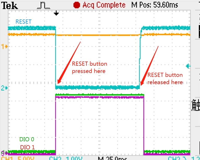
I see the reason.
JN519 this chip has internal pull up resistors which are enabled as default.
So when reset, the chip lost the control of the pins, and the pull up level works, so the output seems high level.
Also, you mean, we have to develop our own board code just like the SDK code?
Tks!
- Mark as New
- Bookmark
- Subscribe
- Mute
- Subscribe to RSS Feed
- Permalink
- Report Inappropriate Content
Hi @wangyilong,
Also, you mean, we have to develop our own board code just like the SDK code?
Your peripheral initialization, and be sure that remove some code depending on the AN that you are working on.
Regards,
Mario
- Mark as New
- Bookmark
- Subscribe
- Mute
- Subscribe to RSS Feed
- Permalink
- Report Inappropriate Content
Hello, Mario
Tks for your reply!
Yes, I found the expansion board definition, but these code locate in SDK.
You mean, I have to rebuild our own SDK to customize our own board? It seems that we are developing a new expansion board?
BTW, it is said in the datasheet that the DIOs will be high impedance input.
But, why it seems high output when reset?
Here is my capture of DIO 0 and DIO 1 when reset:
Tks so much!!

