- NXP Forums
- Product Forums
- General Purpose MicrocontrollersGeneral Purpose Microcontrollers
- i.MX Forumsi.MX Forums
- QorIQ Processing PlatformsQorIQ Processing Platforms
- Identification and SecurityIdentification and Security
- Power ManagementPower Management
- MCX Microcontrollers
- S32G
- S32K
- S32V
- MPC5xxx
- Other NXP Products
- Wireless Connectivity
- S12 / MagniV Microcontrollers
- Powertrain and Electrification Analog Drivers
- Sensors
- Vybrid Processors
- Digital Signal Controllers
- 8-bit Microcontrollers
- ColdFire/68K Microcontrollers and Processors
- PowerQUICC Processors
- OSBDM and TBDML
-
- Solution Forums
- Software Forums
- MCUXpresso Software and ToolsMCUXpresso Software and Tools
- CodeWarriorCodeWarrior
- MQX Software SolutionsMQX Software Solutions
- Model-Based Design Toolbox (MBDT)Model-Based Design Toolbox (MBDT)
- FreeMASTER
- eIQ Machine Learning Software
- Embedded Software and Tools Clinic
- S32 SDK
- S32 Design Studio
- Vigiles
- GUI Guider
- Zephyr Project
- Voice Technology
- Application Software Packs
- Secure Provisioning SDK (SPSDK)
- Processor Expert Software
-
- Topics
- Mobile Robotics - Drones and RoversMobile Robotics - Drones and Rovers
- NXP Training ContentNXP Training Content
- University ProgramsUniversity Programs
- Rapid IoT
- NXP Designs
- SafeAssure-Community
- OSS Security & Maintenance
- Using Our Community
-
-
- Home
- :
- Product Forums
- :
- Wireless Connectivity Knowledge Base
- :
- FRDM-KW41Z Development Platform Errata
FRDM-KW41Z Development Platform Errata
- Subscribe to RSS Feed
- Mark as New
- Mark as Read
- Bookmark
- Subscribe
- Printer Friendly Page
- Report Inappropriate Content
FRDM-KW41Z Development Platform Errata
FRDM-KW41Z Development Platform Errata
The purpose of this document is to communicate known issues with the FRDM-KW41Z development platform. This document applies to all revisions of the FRDM-KW41Z development platform. However, items are divided among their respective revisions and each item may or may not apply to all revisions.
Revision A
The known issues, which may cause confusion for new customers, for revision A are as follows:
1) Incorrect default jumper configuration
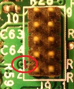
Issue: Jumper, J24, shunt connector does not shunt pins 1 and 2, as noted in the schematic notes.
Impact: Customers will not, by default, be able to put the OpenSDA circuit into bootloader mode.
Workaround: There is currently only one workaround for this issue.
- Move shunt connector on jumper, J24, to shunt pins 1 and 2.
2) Default OpenSDA application may lose serial data
Issue: In certain situations, the serial to USB bridge portion of the default OpenSDA application may not correctly forward serial data. This problem typically only occurs after a POR of a development platform.
Impact: Customers may experience data loss when using the serial to USB converter functionality in their application.
Workaround: There is currently one workaround for this issue.
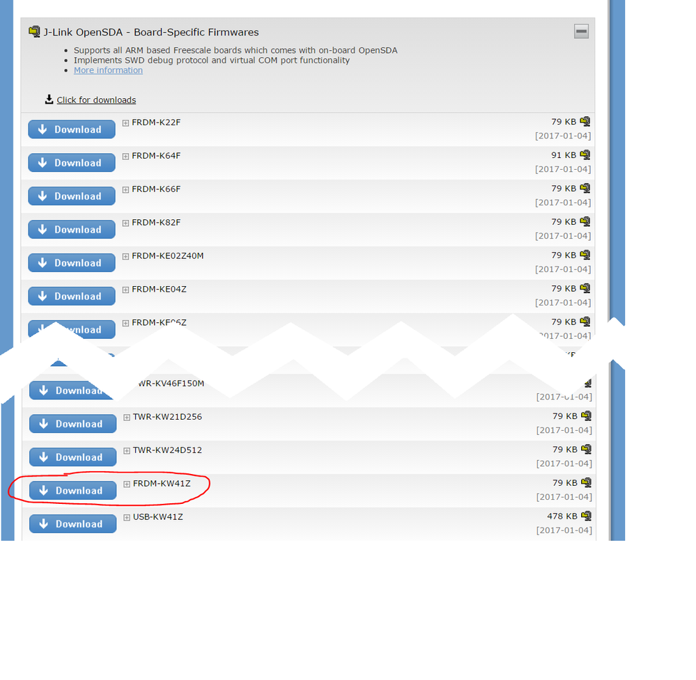
- Update to the latest JLink OpenSDA firmware. To update to this firmware, consult sections 2.1 and 2.2 of the OpenSDA User Guide (found here: http://cache.freescale.com/files/32bit/doc/user_guide/OPENSDAUG.pdf ). The latest JLink OpenSDA firmware can be found here: SEGGER - The Embedded Experts - Downloads - J-Link / J-Trace . (Note: Be sure to select the correct development platform.)
3) Unable to measure correct IDD current when operating in buck mode and P3V3_BRD is disconnected
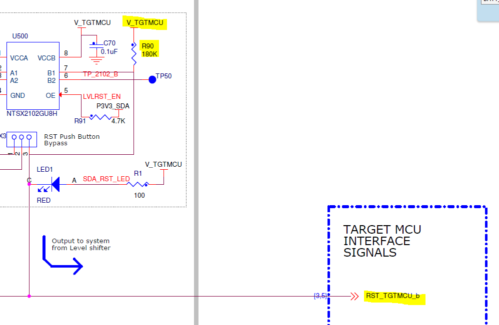
Issue: When configured for buck mode operation and J8 does not have a shunt connector, it is expected that P3V3_BRD will not be powered and thus, board peripherals will not be powered (thermistor, I2C line pull-ups, SPI Flash, Accelerometer, etc,). However it should be noted that in this configuration, P3V3_BRD will be back-powered through resistor R90. R90 is a 180kOhm resistor that connects directly to the MCU reset pin. This R90 also connects to V_TGTMCU which is directly connected to P3V3_BRD through shorting trace SH500. The internal pull-up on the reset pin will, in this case, power P3V3_BRD.
Impact: Customers will not be able to isolate the MCU IDD current from the board peripherals when measuring current in the buck mode configuration. This is a problem mostly when attempting to achieve datasheet IDD current numbers for low power modes in buck mode.
Workaround: There are currently three (3) workarounds for this issue.
- Remove resistor R90.
- Cut shorting trace SH500. Customers should exercise caution when using this workaround. After cutting this short trace, the OpenSDA interface buffers would no longer be powered. Therefore, OpenSDA programming and serial communication will not be possible even when J8 shorting jumper is placed.
- Disable the reset pin in the FOPT field then configure the pin, PTA2, for GPIO output functionality driven low. Customers should exercise caution when implementing this option. The pin, PTA2, could be used as a GPIO in the end application in this configuration, but you would not want to drive PTA2 high while SW1 was directly connected to PTA2 through pins 2 and 3 of jumper J24. In this situation, you potentially short VDD and VSS inadvertently by pressing SW1. If using this workaround, it is recommended to ensure the shorting jumper of J24 is either removed or connected to pins 1 and 2.
4) Incorrect routing of SWD clock for stand-alone debugger configuration
Issue: The signal SWD_CLK_TGTMCU is incorrectly routed to pin 1 of connector J12 instead of pin 4 of the SWD connector, J9.
Impact: With this routing, when the OpenSDA circuit is configured as a stand-alone debugger for debugging other targets (i.e., when J12's shorting trace is cut), the OpenSDA SWD clock will not be able to be present on pin 4 of connector J9. Therefore, the FRDM-KW41Z cannot act as a stand-alone debugger to facilitate debugging other systems.
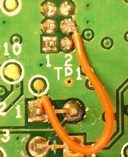
Workaround: There is currently only one workaround for this issue. The workaround is a hardware workaround that requires a cutting tool (such as a modeler's knife), soldering iron, solder, and a spare wire. To implement the workaround, follow these instructions.
- Cut trace J12.
- Cut the trace next to pin 2 and 4 of J9 that connects J9, pin 4 to J12, pin 2. Once this is done, be sure to use a multimeter and ensure there is no electrical connection between J12, pin 2, and J9, pin 4.
- Solder one end of a spare wire to J9, pin 4, and the other end of the spare wire to J12, pin 1. This should be done on the bottom of the board.


