- NXP Forums
- Product Forums
- General Purpose MicrocontrollersGeneral Purpose Microcontrollers
- i.MX Forumsi.MX Forums
- QorIQ Processing PlatformsQorIQ Processing Platforms
- Identification and SecurityIdentification and Security
- Power ManagementPower Management
- MCX Microcontrollers
- S32G
- S32K
- S32V
- MPC5xxx
- Other NXP Products
- Wireless Connectivity
- S12 / MagniV Microcontrollers
- Powertrain and Electrification Analog Drivers
- Sensors
- Vybrid Processors
- Digital Signal Controllers
- 8-bit Microcontrollers
- ColdFire/68K Microcontrollers and Processors
- PowerQUICC Processors
- OSBDM and TBDML
-
- Solution Forums
- Software Forums
- MCUXpresso Software and ToolsMCUXpresso Software and Tools
- CodeWarriorCodeWarrior
- MQX Software SolutionsMQX Software Solutions
- Model-Based Design Toolbox (MBDT)Model-Based Design Toolbox (MBDT)
- FreeMASTER
- eIQ Machine Learning Software
- Embedded Software and Tools Clinic
- S32 SDK
- S32 Design Studio
- Vigiles
- GUI Guider
- Zephyr Project
- Voice Technology
- Application Software Packs
- Secure Provisioning SDK (SPSDK)
- Processor Expert Software
-
- Topics
- Mobile Robotics - Drones and RoversMobile Robotics - Drones and Rovers
- NXP Training ContentNXP Training Content
- University ProgramsUniversity Programs
- Rapid IoT
- NXP Designs
- SafeAssure-Community
- OSS Security & Maintenance
- Using Our Community
-
-
MMA8652FC - Bare metal example project
MMA8652FC - Bare metal example project
Hi Everyone,
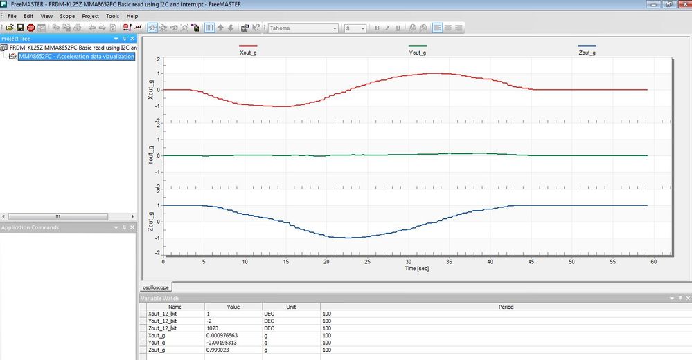
I would like to share here another simple bare-metal example code/demo for the Xtrinsic MMA8652FC digital accelerometer that I have created while working with the Freescale FRDM-KL25Z development platform and FRDM-FXS-MULTI(-B) sensor expansion board. To visualize the acceleration data that are read from the MMA8652FC using an interrupt technique through the I2C interface, I have used the FreeMASTER tool.
This example illustrates:
1. Initialization of the MKL25Z128 MCU (mainly I2C and PORT modules).
2. I2C data write and read operations.
3. Initialization of the accelerometer to achieve the highest resolution.
4. Simple offset calibration based on the AN4069.
5. Output data reading using an interrupt technique.
6. Conversion of the output values from registers 0x01 – 0x06 to real acceleration values in g’s.
7. Visualization of the output values in the FreeMASTER tool.
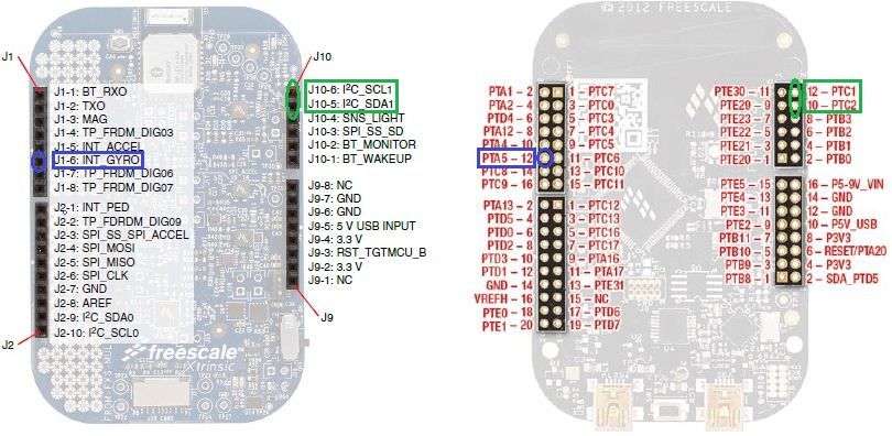
1. As you can see in the FRDM-FXS-MULTI(-B)/FRDM-KL25Z schematics and the image below, I2C signals are routed to the I2C1 module (PTC1 and PTC2 pins) of the KL25Z MCU and the INT1 output is connected to the PTA5 pin (make sure that pin #3 of J4 and pin #2 of J6 connector on the sensor expansion board are connected together). The INT1 output of the MMA8652FC is configured as a push-pull active-low output, so the corresponding PTA5 pin configuration is GPIO with an interrupt on falling edge.
The MCU is, therefore, configured as follows.
void MCU_Init(void)
{
//I2C1 module initialization
SIM_SCGC4 |= SIM_SCGC4_I2C1_MASK; // Turn on clock to I2C1 module
SIM_SCGC5 |= SIM_SCGC5_PORTC_MASK; // Turn on clock to Port C module
PORTC_PCR1 |= PORT_PCR_MUX(0x2); // PTC1 pin is I2C1 SCL line
PORTC_PCR2 |= PORT_PCR_MUX(0x2); // PTC2 pin is I2C1 SDA line
I2C1_F |= I2C_F_ICR(0x14); // SDA hold time = 2.125us, SCL start hold time = 4.25us, SCL stop hold time = 5.125us
I2C1_C1 |= I2C_C1_IICEN_MASK; // Enable I2C1 module
//Configure the PTA5 pin (connected to the INT1 of the MMA8652FC) for falling edge interrupts
SIM_SCGC5 |= SIM_SCGC5_PORTA_MASK; // Turn on clock to Port A module
PORTA_PCR5 |= (0|PORT_PCR_ISF_MASK| // Clear the interrupt flag
PORT_PCR_MUX(0x1)| // PTA5 is configured as GPIO
PORT_PCR_IRQC(0xA)); // PTA5 is configured for falling edge interrupts
//Enable PORTA interrupt on NVIC
NVIC_ICPR |= 1 << ((INT_PORTA - 16)%32);
NVIC_ISER |= 1 << ((INT_PORTA - 16)%32);
}
2. The 7-bit I2C address of the MMA8652FC is fixed value 0x1D. As shown above, the SCL line is connected to the PTC1 pin and SDA line to the PTC2 pin. The I2C clock frequency is 125 kHz.
The screenshot below shows the write operation which writes the value 0x39 to the CTRL_REG1 (0x2A).
And here is the single byte read from the WHO_AM_I register 0x0D. As you can see, it returns the correct value 0x4A.
Multiple bytes of data can be read from sequential registers after each MMA8652FC acknowledgment (AK) is received until a no acknowledge (NAK) occurs from the KL25Z followed by a stop condition (SP) signaling an end of transmission. A burst read of 6 bytes from registers 0x01 to 0x06 is shown below. It also shows how the INT1 pin is automatically deasserted by reading the acceleration output data.
3. At the beginning of the initialization, all registers are reset to their default values by setting the RST bit of the CTRL_REG2 register. The dynamic range is set to ±2g and to achieve the highest resolution, the lowest ODR (1.56Hz) and the High Resolution mode are selected (more details in AN4075). The DRDY interrupt is enabled and routed to the INT1 interrupt pin that is configured to be a push-pull, active-low output.
void MMA8652FC_Init (void)
{
I2C_WriteRegister(MMA8652FC_I2C_ADDRESS, CTRL_REG2, 0x40); // Reset all registers to POR values
Pause(0x631); // ~1ms delay
I2C_WriteRegister(MMA8652FC_I2C_ADDRESS, XYZ_DATA_CFG_REG, 0x00); // +/-2g range with ~0.977mg/LSB
I2C_WriteRegister(MMA8652FC_I2C_ADDRESS, CTRL_REG2, 0x02); // High Resolution mode
I2C_WriteRegister(MMA8652FC_I2C_ADDRESS, CTRL_REG3, 0x00); // Push-pull, active low interrupt
I2C_WriteRegister(MMA8652FC_I2C_ADDRESS, CTRL_REG4, 0x01); // Enable DRDY interrupt
I2C_WriteRegister(MMA8652FC_I2C_ADDRESS, CTRL_REG5, 0x01); // DRDY interrupt routed to INT1 - PTA5
I2C_WriteRegister(MMA8652FC_I2C_ADDRESS, CTRL_REG1, 0x39); // ODR = 1.56Hz, Active mode
}
4. A simple offset calibration method is implemented according to the AN4069.
void MMA8652FC_Calibration (void)
{
char X_offset, Y_offset, Z_offset;
DataReady = 0;
while (!DataReady){} // Is a first set of data ready?
DataReady = 0;
I2C_WriteRegister(MMA8652FC_I2C_ADDRESS, CTRL_REG1, 0x00); // Standby mode
I2C_ReadMultiRegisters(MMA8652FC_I2C_ADDRESS, OUT_X_MSB_REG, 6, AccelData); // Read data output registers 0x01-0x06
Xout_12_bit = ((short) (AccelData[0]<<8 | AccelData[1])) >> 4; // Compute 12-bit X-axis acceleration output value
Yout_12_bit = ((short) (AccelData[2]<<8 | AccelData[3])) >> 4; // Compute 12-bit Y-axis acceleration output value
Zout_12_bit = ((short) (AccelData[4]<<8 | AccelData[5])) >> 4; // Compute 12-bit Z-axis acceleration output value
X_offset = Xout_12_bit / 2 * (-1); // Compute X-axis offset correction value
Y_offset = Yout_12_bit / 2 * (-1); // Compute Y-axis offset correction value
Z_offset = (Zout_12_bit - SENSITIVITY_2G) / 2 * (-1); // Compute Z-axis offset correction value
I2C_WriteRegister(MMA8652FC_I2C_ADDRESS, OFF_X_REG, X_offset);
I2C_WriteRegister(MMA8652FC_I2C_ADDRESS, OFF_Y_REG, Y_offset);
I2C_WriteRegister(MMA8652FC_I2C_ADDRESS, OFF_Z_REG, Z_offset);
I2C_WriteRegister(MMA8652FC_I2C_ADDRESS, CTRL_REG1, 0x39); // Active mode again
}
5. In the ISR, only the interrupt flag is cleared and the DataReady variable is set to indicate the arrival of new data.
void PORTA_IRQHandler()
{
PORTA_PCR5 |= PORT_PCR_ISF_MASK; // Clear the interrupt flag
DataReady = 1;
}
6. The output values from accelerometer registers 0x01 – 0x06 are first converted to signed 12-bit values and afterwards to real values in g’s.
if (DataReady) // Is a new set of data ready?
{
DataReady = 0;
I2C_ReadMultiRegisters(MMA8652FC_I2C_ADDRESS, OUT_X_MSB_REG, 6, AccelData); // Read data output registers 0x01-0x06
// 12-bit accelerometer data
Xout_12_bit = ((short) (AccelData[0]<<8 | AccelData[1])) >> 4; // Compute 12-bit X-axis acceleration output value
Yout_12_bit = ((short) (AccelData[2]<<8 | AccelData[3])) >> 4; // Compute 12-bit Y-axis acceleration output value
Zout_12_bit = ((short) (AccelData[4]<<8 | AccelData[5])) >> 4; // Compute 12-bit Z-axis acceleration output value
// Accelerometer data converted to g's
Xout_g = ((float) Xout_12_bit) / SENSITIVITY_2G; // Compute X-axis output value in g's
Yout_g = ((float) Yout_12_bit) / SENSITIVITY_2G; // Compute Y-axis output value in g's
Zout_g = ((float) Zout_12_bit) / SENSITIVITY_2G; // Compute Z-axis output value in g's
}
7. The calculated values can be watched in the "Variables" window on the top right of the Debug perspective or in the FreeMASTER application. To open and run the FreeMASTER project, install the FreeMASTER application and FreeMASTER Communication Driver.
Attached you can find the complete source code written in the CW for MCU's (Eclipse IDE) including the FreeMASTER project.
If there are any questions regarding this simple application, do not hesitate to ask below. Your feedback or suggestions are also welcome.
Regards,
Tomas
Hello Tomas,
I found this project very helpful, and I follow it to configure my MMA8652FC.
But I want to work with it using only 8 bits.
I'm able to configure it to use only 8 bits, and I get the Xout_8_bit, Yout_8_bit, Zout_8_bit. But how do I calculate the offset values?
X_offset_8_bit = ?
Y_offset_8_bit = ?
Z_offset_8_bit = ?
Can you help me?
Thanks.
Regards,
Sérgio
Hello Sérgio,
SENSITIVITY_2G_8bits 64
SENSITIVITY_4G_8bits 32
SENSITIVITY_8G_8bits 16
±2g:
X_offset_2G_8_bit = Xout_8_bit * 8 * (-1);
Y_offset_2G_8_bit = Yout_8_bit * 8 * (-1);
Z_offset_2G_8_bit = (Zout_8_bit - SENSITIVITY_2G_8bits) * 8 * (-1);
±4g:
X_offset_4G_8_bit = Xout_8_bit * 16 * (-1);
Y_offset_4G_8_bit = Yout_8_bit * 16 * (-1);
Z_offset_4G_8_bit = (Zout_8_bit - SENSITIVITY_4G_8bits) * 16 * (-1);
±8g:
X_offset_8G_8_bit = Xout_8_bit * 32 * (-1);
Y_offset_8G_8_bit = Yout_8_bit * 32 * (-1);
Z_offset_8G_8_bit = (Zout_8_bit - SENSITIVITY_8G_8bits) * 32 * (-1);
Best regards,
Tomas
Hello Tomas,
Thanks for all the help.
Regards,
Sérgio


