
- Forums
- Product Forums
- General Purpose MicrocontrollersGeneral Purpose Microcontrollers
- i.MX Forumsi.MX Forums
- QorIQ Processing PlatformsQorIQ Processing Platforms
- Identification and SecurityIdentification and Security
- Power ManagementPower Management
- Wireless ConnectivityWireless Connectivity
- RFID / NFCRFID / NFC
- Advanced AnalogAdvanced Analog
- Neural Processing UnitsNeural Processing Units
- MCX Microcontrollers
- S32G
- S32K
- S32V
- MPC5xxx
- Other NXP Products
- S12 / MagniV Microcontrollers
- Powertrain and Electrification Analog Drivers
- Sensors
- Vybrid Processors
- Digital Signal Controllers
- 8-bit Microcontrollers
- ColdFire/68K Microcontrollers and Processors
- PowerQUICC Processors
- OSBDM and TBDML
- S32M
- S32Z/E
-
- Solution Forums
- Software Forums
- MCUXpresso Software and ToolsMCUXpresso Software and Tools
- CodeWarriorCodeWarrior
- MQX Software SolutionsMQX Software Solutions
- Model-Based Design Toolbox (MBDT)Model-Based Design Toolbox (MBDT)
- FreeMASTER
- eIQ Machine Learning Software
- Embedded Software and Tools Clinic
- S32 SDK
- S32 Design Studio
- GUI Guider
- Zephyr Project
- Voice Technology
- Application Software Packs
- Secure Provisioning SDK (SPSDK)
- Processor Expert Software
- Generative AI & LLMs
-
- Topics
- Mobile Robotics - Drones and RoversMobile Robotics - Drones and Rovers
- NXP Training ContentNXP Training Content
- University ProgramsUniversity Programs
- Rapid IoT
- NXP Designs
- SafeAssure-Community
- OSS Security & Maintenance
- Using Our Community
-
- Cloud Lab Forums
-
- Knowledge Bases
- ARM Microcontrollers
- i.MX Processors
- Identification and Security
- Model-Based Design Toolbox (MBDT)
- QorIQ Processing Platforms
- S32 Automotive Processing Platform
- Wireless Connectivity
- CodeWarrior
- MCUXpresso Suite of Software and Tools
- MQX Software Solutions
- RFID / NFC
- Advanced Analog
- Neural Processing Units
-
- NXP Tech Blogs
- Home
- :
- QorIQ Processing Platforms
- :
- QorIQ
- :
- T2080 Reference Board
T2080 Reference Board
- Subscribe to RSS Feed
- Mark Topic as New
- Mark Topic as Read
- Float this Topic for Current User
- Bookmark
- Subscribe
- Mute
- Printer Friendly Page
T2080 Reference Board
- Mark as New
- Bookmark
- Subscribe
- Mute
- Subscribe to RSS Feed
- Permalink
- Report Inappropriate Content
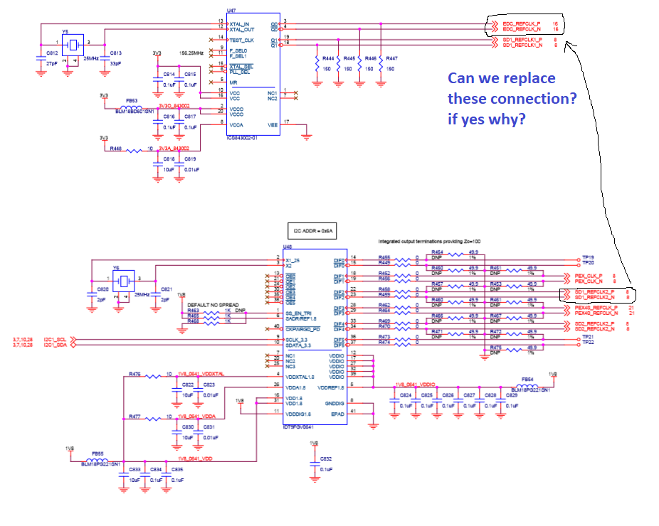
Hello,
Currently i am working on the device is based t2080 processor.
In the design i am only using one Ethernet phy i.e. RTL8211E-VB.
As i am not using 10G EDC PHY CS4315, can i connect the SD1_REFCLK2 and SD1_REFCLK2 to U47 ICS843002-01? If yes, then why it is not connected in the reference design?
To understand better, i am enclosing the image for the same.
Waiting for your reply,
Regards
Hemant
- Mark as New
- Bookmark
- Subscribe
- Mute
- Subscribe to RSS Feed
- Permalink
- Report Inappropriate Content
Please refer to the following picture:

to realize that SD1_REFCLK1_P/N is 156.25MHz and SD1_REFCLK2_P/N is 100MHz
- Mark as New
- Bookmark
- Subscribe
- Mute
- Subscribe to RSS Feed
- Permalink
- Report Inappropriate Content
In the image that you have shared above show SD2_REFCLK1_P/N AND SD2_REFCLK2_P/N are coming from IDT9FGV0641 but in the reference design SD2_REFCLK2_P/N is coming out from IDT9FGV0641 while SD1_REFCLK2_P/N is coming from ICS859S0212I?
If i connect both SD2_REFCLK1_P/N AND SD2_REFCLK2_P/N to IDT9FGV0641, is it going to work?
As i can see in the schematic that to diff. pair are free in IDT9FGV0641?
Waiting for your reply!!
- Mark as New
- Bookmark
- Subscribe
- Mute
- Subscribe to RSS Feed
- Permalink
- Report Inappropriate Content
It is not clear what are you intended to do.
Please provide the proposed block diagram and corresponding SerDes1 & 2 protocols which you plan to use.
- Mark as New
- Bookmark
- Subscribe
- Mute
- Subscribe to RSS Feed
- Permalink
- Report Inappropriate Content
I am not using any kind of the PCIe connector in my design,
and according to picture shared by you both SD2_REFCLK1_P/N and SD2_REFCLK2_P/N both having frequency of 100MHz.
my question is whether i can connect both the SD2_REFCLK1_P/N and SD2_REFCLK2_P to IDT9FGV0641 while eliminating the need of ICS859S0212I IC ?
Attaching the image for your reference?
Regards
Hemant

- Mark as New
- Bookmark
- Subscribe
- Mute
- Subscribe to RSS Feed
- Permalink
- Report Inappropriate Content
Please draw and provide the proposed clocking block diagram and corresponding SerDes1 & 2 protocols which you plan to use.
- Mark as New
- Bookmark
- Subscribe
- Mute
- Subscribe to RSS Feed
- Permalink
- Report Inappropriate Content
Please ignore the above shared image as it was wrong.
Attaching the final proposed clocking diagram.

- Mark as New
- Bookmark
- Subscribe
- Mute
- Subscribe to RSS Feed
- Permalink
- Report Inappropriate Content
Which SerDes1 & 2 protocols you plan to use?
- Mark as New
- Bookmark
- Subscribe
- Mute
- Subscribe to RSS Feed
- Permalink
- Report Inappropriate Content
Serdes 2
- Mark as New
- Bookmark
- Subscribe
- Mute
- Subscribe to RSS Feed
- Permalink
- Report Inappropriate Content
SerDes Protocols:

etc....
- Mark as New
- Bookmark
- Subscribe
- Mute
- Subscribe to RSS Feed
- Permalink
- Report Inappropriate Content
my question is related to clocking. attaching the same for your reference.
Please check and tell me whether the connection that i have made are correct or not as per t2080 reference design?

- Mark as New
- Bookmark
- Subscribe
- Mute
- Subscribe to RSS Feed
- Permalink
- Report Inappropriate Content
T2080RDB supports only SRDS_PRTCL_S1=0x66 and SRDS_PRTCL_S2=0x15.
Are the same used in your design?
- Mark as New
- Bookmark
- Subscribe
- Mute
- Subscribe to RSS Feed
- Permalink
- Report Inappropriate Content
Showing the proposed clocking diagram. Please check and let me know what you think?

- Mark as New
- Bookmark
- Subscribe
- Mute
- Subscribe to RSS Feed
- Permalink
- Report Inappropriate Content
Please ignore the above shared image as it was wrong.
Attaching the final proposed clocking diagram.
