
- Forums
- Product Forums
- General Purpose MicrocontrollersGeneral Purpose Microcontrollers
- i.MX Forumsi.MX Forums
- QorIQ Processing PlatformsQorIQ Processing Platforms
- Identification and SecurityIdentification and Security
- Power ManagementPower Management
- Wireless ConnectivityWireless Connectivity
- RFID / NFCRFID / NFC
- Advanced AnalogAdvanced Analog
- Neural Processing UnitsNeural Processing Units
- MCX Microcontrollers
- S32G
- S32K
- S32V
- MPC5xxx
- Other NXP Products
- S12 / MagniV Microcontrollers
- Powertrain and Electrification Analog Drivers
- Sensors
- Vybrid Processors
- Digital Signal Controllers
- 8-bit Microcontrollers
- ColdFire/68K Microcontrollers and Processors
- PowerQUICC Processors
- OSBDM and TBDML
- S32M
- S32Z/E
-
- Solution Forums
- Software Forums
- MCUXpresso Software and ToolsMCUXpresso Software and Tools
- CodeWarriorCodeWarrior
- MQX Software SolutionsMQX Software Solutions
- Model-Based Design Toolbox (MBDT)Model-Based Design Toolbox (MBDT)
- FreeMASTER
- eIQ Machine Learning Software
- Embedded Software and Tools Clinic
- S32 SDK
- S32 Design Studio
- GUI Guider
- Zephyr Project
- Voice Technology
- Application Software Packs
- Secure Provisioning SDK (SPSDK)
- Processor Expert Software
- Generative AI & LLMs
-
- Topics
- Mobile Robotics - Drones and RoversMobile Robotics - Drones and Rovers
- NXP Training ContentNXP Training Content
- University ProgramsUniversity Programs
- Rapid IoT
- NXP Designs
- SafeAssure-Community
- OSS Security & Maintenance
- Using Our Community
-
- Cloud Lab Forums
-
- Knowledge Bases
- ARM Microcontrollers
- i.MX Processors
- Identification and Security
- Model-Based Design Toolbox (MBDT)
- QorIQ Processing Platforms
- S32 Automotive Processing Platform
- Wireless Connectivity
- CodeWarrior
- MCUXpresso Suite of Software and Tools
- MQX Software Solutions
- RFID / NFC
- Advanced Analog
- Neural Processing Units
-
- NXP Tech Blogs
- Home
- :
- 製品フォーラム
- :
- PowerQUICCプロセッサ
- :
- Re: P2020 Processor GPCM with DLL Bypass Read/Write Timing
P2020 Processor GPCM with DLL Bypass Read/Write Timing
- RSS フィードを購読する
- トピックを新着としてマーク
- トピックを既読としてマーク
- このトピックを現在のユーザーにフロートします
- ブックマーク
- 購読
- ミュート
- 印刷用ページ
- 新着としてマーク
- ブックマーク
- 購読
- ミュート
- RSS フィードを購読する
- ハイライト
- 印刷
- 不適切なコンテンツを報告
When looking at the P2020 QorIQ Integrated Processor Reference Manual (Rev. 2, 12/2012), I notice that when the local bus is in bypass mode, eLBC drives new address, data, and control signals effectively on falling edges of LCLK, but continues to sample synchronous read data on rising edges of LCLK to maximize the set-up margin for reads. However, the precise timing relationship between TA signal and read-write signal is not clearly stated.
I need to do an accurate timing analysis, but I don't know the specific timing relationship between TA signal and read-write signal, and which rising edge of LCLK is the sampling point for reading data when TA signal is asserted.
The register settings in my design are as follows:
BR:0xd0001001
OR:0xffff0ef5
Any help would be much appreciated.
Thanks.
解決済! 解決策の投稿を見る。
- 新着としてマーク
- ブックマーク
- 購読
- ミュート
- RSS フィードを購読する
- ハイライト
- 印刷
- 不適切なコンテンツを報告
Your understanding is generally correct.
Please consider that it is convenient to create new Community question/thread for the new question.
- 新着としてマーク
- ブックマーク
- 購読
- ミュート
- RSS フィードを購読する
- ハイライト
- 印刷
- 不適切なコンテンツを報告
Your understanding is generally correct.
Please consider that it is convenient to create new Community question/thread for the new question.
- 新着としてマーク
- ブックマーク
- 購読
- ミュート
- RSS フィードを購読する
- ハイライト
- 印刷
- 不適切なコンテンツを報告
Thank you very much.
- 新着としてマーク
- ブックマーク
- 購読
- ミュート
- RSS フィードを購読する
- ハイライト
- 印刷
- 不適切なコンテンツを報告
Please refer to the P2020 QorIQ Integrated Processor Hardware Specifications, 2.12.2.3 Local Bus AC Timing Specifications for PLL Bypass Mode:
https://www.nxp.com/webapp/Download?colCode=P2020EC&location=null
- 新着としてマーク
- ブックマーク
- 購読
- ミュート
- RSS フィードを購読する
- ハイライト
- 印刷
- 不適切なコンテンツを報告
I have read the p2020ec, but I still haven't figured out the exact timing relationship between the sampling point of reading data and the reading signal. At the same time, the time when writing data becomes invalid is related to the accurate timing of writing signal
Can you give me a further explanation on the attached figure?
Thank you.
- 新着としてマーク
- ブックマーク
- 購読
- ミュート
- RSS フィードを購読する
- ハイライト
- 印刷
- 不適切なコンテンツを報告
P2020 QorIQ Integrated Processor Reference Manual, 12.4.1.7 PLL Bypass mode:
"In PLL bypass mode, eLBC drives new address, data, and control signals effectively on falling edges of LCLK, but continues to sample synchronous read data on rising edges of LCLK to maximize the set-up margin for reads."
In the P2020 QorIQ Integrated Processor Hardware Specifications, 2.12.2.3 Local Bus AC Timing Specifications for PLL Bypass Mode:

- 新着としてマーク
- ブックマーク
- 購読
- ミュート
- RSS フィードを購読する
- ハイライト
- 印刷
- 不適切なコンテンツを報告
Thank you for your reply.
According to your description, the sampling point for reading data should be the rising edge of lclk before the LOE is invalid, and at the next falling edge of lclk, LOE becomes invalid. Is my description right?
In addition, how about write timing?
- 新着としてマーク
- ブックマーク
- 購読
- ミュート
- RSS フィードを購読する
- ハイライト
- 印刷
- 不適切なコンテンツを報告
> Is my description right?
Yes.
> In addition, how about write timing?
Please refer to the Figure 40 in the P2020 QorIQ Integrated Processor Hardware Specifications, 2.12.2.3 Local Bus AC Timing Specifications for PLL Bypass Mode.
- 新着としてマーク
- ブックマーク
- 購読
- ミュート
- RSS フィードを購読する
- ハイライト
- 印刷
- 不適切なコンテンツを報告
In my design, OR register is set as follows:
AM(0~16) | 17~18) | BCTLD(19) | CSNT(20) | ACS(21~22) | XACS(23) |
0x1fff8 | 00 | 0 | 1 | 11 | 0 |
SCY(24~27) | SETA(28) | TRLX(29) | EHTR(30) | EAD(31) |
|
1111 | 0 | 1 | 1 | 0 |
|
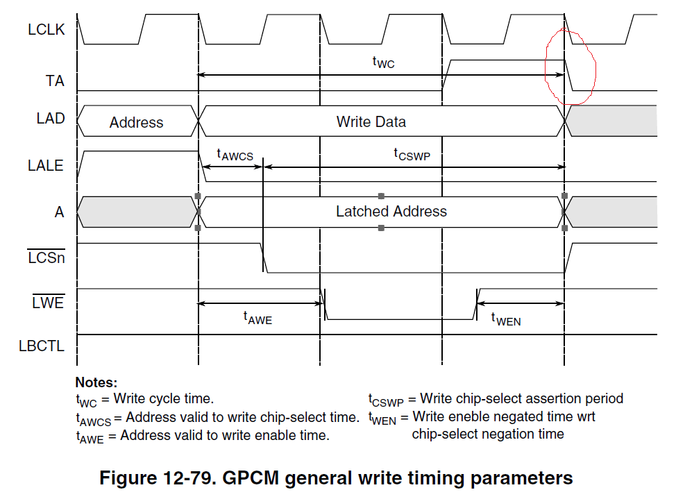
According to P2020RM (Rev. 2, 12/2012) Table 12-191. GPCM write control signal timing parameters as follows:
TRLX | XACS | ACS | CSNT | tAWCS | tCSWP | tAWE | tWEN | tWC |
1 | 0 | 11 | 1 | 1.5 | 1.25+2* SCY | 2 | 0 | 2.75+2* SCY |
But because TRLX = 1, so LCSn and LWE signals are negated one cycle earlier during Writes. The parameters in the above table will change to the following:
TRLX | XACS | ACS | CSNT | tAWCS | tCSWP | tAWE | tWEN | tWC |
1 | 0 | 11 | 1 | 1.5 | 0.25+2* SCY | 2 | 1 | 2.75+2* SCY |
According to the above description, I have drawn the following timing diagram:

Is my description and timing diagram right?
I will be looking forward to your reply.
- 新着としてマーク
- ブックマーク
- 購読
- ミュート
- RSS フィードを購読する
- ハイライト
- 印刷
- 不適切なコンテンツを報告
You need to use timing data from the corresponding row of the "Table 12-191. GPCM write control signal timing" without any modification.
- 新着としてマーク
- ブックマーク
- 購読
- ミュート
- RSS フィードを購読する
- ハイライト
- 印刷
- 不適切なコンテンツを報告
According to your help and my understanding of the P2020RM, I think the reading and writing sequence is as follows:
PLL bypass read timing:
The sampling point for reading data should be the rising edge of lclk before the LOE/LCS is invalid. This time is determined by the parameter tCSRP.
PLL bypass write timing:
Write data is invalid at the end of the tWC. This time is determined by the parameter tWC.
Is my understanding right?
I have another question:
As described in P2020RM, LCSn (only if ACS is not equal to 00) and LWE signals are negated one cycle earlier during Writes when TRLX is 1.
The write sequence will change from Figure 1 to figure 2?

Figure 1

Figure 2
- 新着としてマーク
- ブックマーク
- 購読
- ミュート
- RSS フィードを購読する
- ハイライト
- 印刷
- 不適切なコンテンツを報告
If I use timing data from the corresponding row of the "Table 12-191. GPCM write control signal timing" without any modification.
TRLX | XACS | ACS | CSNT | tAWCS | tCSWP | tAWE | tWEN | tWC |
1 | 0 | 11 | 1 | 1.5 | 1.25+2* SCY | 2 | 0 | 2.75++2* SCY |
Write timing diagram as following:

If it is the above timing, write data and write signal are invalid at the same time. so the hold time of write data will be insufficient.
And according to your comment, I am confused about the following description in P2020RM:
TRLX is 1:
Relaxed timing on the following parameters:
• Adds an additional cycle between the address and control signals (only if ACS is not equal to
00).
• Doubles the number of wait states specified by SCY, providing up to 30 wait states.
• Works in conjunction with EHTR to extend hold time on read accesses.
• LCSn (only if ACS is not equal to 00) and LWE signals are negated one cycle earlier during
Writes
- 新着としてマーク
- ブックマーク
- 購読
- ミュート
- RSS フィードを購読する
- ハイライト
- 印刷
- 不適切なコンテンツを報告
If Twen = 0, is writing data and writing signal invalid at the same time?