
- NXP Forums
- Product Forums
- General Purpose MicrocontrollersGeneral Purpose Microcontrollers
- i.MX Forumsi.MX Forums
- QorIQ Processing PlatformsQorIQ Processing Platforms
- Identification and SecurityIdentification and Security
- Power ManagementPower Management
- MCX Microcontrollers
- S32G
- S32K
- S32V
- MPC5xxx
- Other NXP Products
- Wireless Connectivity
- S12 / MagniV Microcontrollers
- Powertrain and Electrification Analog Drivers
- Sensors
- Vybrid Processors
- Digital Signal Controllers
- 8-bit Microcontrollers
- ColdFire/68K Microcontrollers and Processors
- PowerQUICC Processors
- OSBDM and TBDML
-
- Solution Forums
- Software Forums
- MCUXpresso Software and ToolsMCUXpresso Software and Tools
- CodeWarriorCodeWarrior
- MQX Software SolutionsMQX Software Solutions
- Model-Based Design Toolbox (MBDT)Model-Based Design Toolbox (MBDT)
- FreeMASTER
- eIQ Machine Learning Software
- Embedded Software and Tools Clinic
- S32 SDK
- S32 Design Studio
- Vigiles
- GUI Guider
- Zephyr Project
- Voice Technology
- Application Software Packs
- Secure Provisioning SDK (SPSDK)
- Processor Expert Software
-
- Topics
- Mobile Robotics - Drones and RoversMobile Robotics - Drones and Rovers
- NXP Training ContentNXP Training Content
- University ProgramsUniversity Programs
- Rapid IoT
- NXP Designs
- SafeAssure-Community
- OSS Security & Maintenance
- Using Our Community
-
-
- Home
- :
- Product Forums
- :
- OSBDM and TBDML
- :
- Kinetis KL05 secured ? How to unlock with USBDM ?
Kinetis KL05 secured ? How to unlock with USBDM ?
- Subscribe to RSS Feed
- Mark Topic as New
- Mark Topic as Read
- Float this Topic for Current User
- Bookmark
- Subscribe
- Mute
- Printer Friendly Page
Kinetis KL05 secured ? How to unlock with USBDM ?
- Mark as New
- Bookmark
- Subscribe
- Mute
- Subscribe to RSS Feed
- Permalink
- Report Inappropriate Content
Hello everybody, and particularly PGO,
I have already posted in Kinetis category on the forum, but no one seems to use the USBDM there ! :smileyhappy: Here is my problem :
I have just bought some KL05 devices from Freescale and try to program them with an USBDM (based on "USBDM_SWD_JS16CWJ.pdf" schematic), but it seems that the devices are secured when they are new.... ?
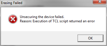
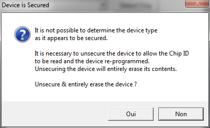
With the standalone ARM programmer published by PGO I get a warning saying that the device is secured ("ARM Programmer - Device is Secured.PNG"), I click "Yes" to mass erase the microcontroller but then it fails ("ARM Programmer - Erasing Failed.PNG").
With CodeWarrior 10.4 I get a warning saying that the device is secured ("CodeWarrior - Device is secured.PNG"), I click "Yes" to mass erase the microcontroller but then it fails ("CodeWarrior - Problem occurred.PNG").
Do you know how to unlock the KL05 devices ? It will be really great if it is possible to do it with the USBDM... if not, maybe with another tool ... ?
I'm using the last USBDM version.
Thanks for your feedbacks,
Best Regards,
Joel Guittet
PS : link to the other post on the forum : Kinetis KL05 secured ? How to unlock with USBDM ?
- Mark as New
- Bookmark
- Subscribe
- Mute
- Subscribe to RSS Feed
- Permalink
- Report Inappropriate Content
Hi Guittet,
USBDM should be able to unsecure a Kinetis device providing the unsecure function has not been disabled. There may be some connection problems due to watchdog issues etc but I have not seen these with an entirely blank chip. There are issues if the device has been programmed with invalid information.
I don't have a pristine device to test with. The only devices I have, have been previously programmed. The best test I can do is to erase a chip and re-program it to a secured state. USBDM works OK with this. I believe Freescale distribute the chips in an unsecured condition.
I'm unsure what situation is causing the program.
If you have the patience you can use the attached script to try to see what is going wrong with the mass erase of the device.
- Save the attached text as a TCL script try.tcl in the USBDM installation root directory (.../USBDM 4.10.5).
- Start the USBDM TCL Interpreter from the USBDM menu
- Type source try.tcl
- It should produce one of the results commented in the script below. The second result indicates the chip is failing to unsecure (rather than some bug).
Bye
PS. The forum doesn't like the attachment - which is not surprising since it's a script that could potentially do anything to your machine!
I've added it inline - you can assess the risk to running it ![]() .
.
openbdm
settarget arm
source devicedata/arm/Kinetis-KLxx-flash-scripts.tcl
massEraseTarget
closebdm


# Expected successful results for a secured chip (mass erase not disabled)
#
# Found 1 devices
# USBDM DLL Version = 4.10.5.0
# BDM Version = HW=97, SW=4A
# USBDM DLL Version = 4.10.5.0
# BDM Version = HW=97, SW=4A
# :setTarget ARM
# bytesex => Little-endian
# :pinSet 0x8
# :rCreg r=0x1000004(MDM_AP.Control)->0x00000000
# :wCreg r=0x1000004(MDM_AP.Control)<-0x00000019
# :wCreg r=0x1000004(MDM_AP.Control)<-0x00000011
# :rCreg r=0x1000004(MDM_AP.Control)->0x00000010
# :wCreg r=0x1000004(MDM_AP.Control)<-0x00000000
# :reset 0x08(SOFTWARE, SPECIAL)
# %

# Expected unsuccessful results for a secured chip (mass erase disabled)
# % source try.tcl
# Found 1 devices
# USBDM DLL Version = 4.10.5.0
# BDM Version = HW=97, SW=4A
# USBDM DLL Version = 4.10.5.0
# BDM Version = HW=97, SW=4A
# :setTarget ARM
# bytesex => Little-endian
# :pinSet 0x8
# :rCreg r=0x1000004(MDM_AP.Control)->0x00000000
# :wCreg r=0x1000004(MDM_AP.Control)<-0x00000019
# :wCreg r=0x1000004(MDM_AP.Control)<-0x00000011
# :rCreg r=0x1000004(MDM_AP.Control)->0x00000001
# :rCreg r=0x1000004(MDM_AP.Control)->0x00000001
# :rCreg r=0x1000004(MDM_AP.Control)->0x00000001
# :rCreg r=0x1000004(MDM_AP.Control)->0x00000001
# :rCreg r=0x1000004(MDM_AP.Control)->0x00000001
# :rCreg r=0x1000004(MDM_AP.Control)->0x00000001
# :rCreg r=0x1000004(MDM_AP.Control)->0x00000001
# :rCreg r=0x1000004(MDM_AP.Control)->0x00000001
# :rCreg r=0x1000004(MDM_AP.Control)->0x00000001
# :rCreg r=0x1000004(MDM_AP.Control)->0x00000001
# :rCreg r=0x1000004(MDM_AP.Control)->0x00000001
# :wCreg r=0x1000004(MDM_AP.Control)<-0x00000001
# :reset 0x08(SOFTWARE, SPECIAL)
# Flash mass erase failed
# %
!
- Mark as New
- Bookmark
- Subscribe
- Mute
- Subscribe to RSS Feed
- Permalink
- Report Inappropriate Content
here's the thing now
i does as this website said
http://www.deskdecode.com/bad-pool-header/
and now my system wont able to start
what to do now does anybody knows something
- Mark as New
- Bookmark
- Subscribe
- Mute
- Subscribe to RSS Feed
- Permalink
- Report Inappropriate Content
pgo wrote:
Hi Guittet,
USBDM should be able to unsecure a Kinetis device providing the unsecure function has not been disabled. There may be some connection problems due to watchdog issues etc but I have not seen these with an entirely blank chip. There are issues if the device has been programmed with invalid information.
I don't have a pristine device to test with. The only devices I have, have been previously programmed. The best test I can do is to erase a chip and re-program it to a secured state. USBDM works OK with this. I believe Freescale distribute the chips in an unsecured condition.
I'm unsure what situation is causing the program.
If you have the patience you can use the attached script to try to see what is going wrong with the mass erase of the device.
- Save the attached text as a TCL script try.tcl in the USBDM installation root directory (.../USBDM 4.10.5).
- Start the USBDM TCL Interpreter from the USBDM menu
- Type source try.tcl
- It should produce one of the results commented in the script below. The second result indicates the chip is failing to unsecure (rather than some bug).
Bye
PS. The forum doesn't like the attachment - which is not surprising since it's a script that could potentially do anything to your machine!
I've added it inline - you can assess the risk to running it .
- openbdm
- settarget arm
- source devicedata/arm/Kinetis-KLxx-flash-scripts.tcl
- massEraseTarget
- closebdm
- # Expected successful results for a secured chip (mass erase not disabled)
- #
- # Found 1 devices
- # USBDM DLL Version = 4.10.5.0
- # BDM Version = HW=97, SW=4A
- # USBDM DLL Version = 4.10.5.0
- # BDM Version = HW=97, SW=4A
- # :setTarget ARM
- # bytesex => Little-endian
- # :pinSet 0x8
- # :rCreg r=0x1000004(MDM_AP.Control)->0x00000000
- # :wCreg r=0x1000004(MDM_AP.Control)<-0x00000019
- # :wCreg r=0x1000004(MDM_AP.Control)<-0x00000011
- # :rCreg r=0x1000004(MDM_AP.Control)->0x00000010
- # :wCreg r=0x1000004(MDM_AP.Control)<-0x00000000
- # :reset 0x08(SOFTWARE, SPECIAL)
- # %
- # Expected unsuccessful results for a secured chip (mass erase disabled)
- # % source try.tcl
- # Found 1 devices
- # USBDM DLL Version = 4.10.5.0
- # BDM Version = HW=97, SW=4A
- # USBDM DLL Version = 4.10.5.0
- # BDM Version = HW=97, SW=4A
- # :setTarget ARM
- # bytesex => Little-endian
- # :pinSet 0x8
- # :rCreg r=0x1000004(MDM_AP.Control)->0x00000000
- # :wCreg r=0x1000004(MDM_AP.Control)<-0x00000019
- # :wCreg r=0x1000004(MDM_AP.Control)<-0x00000011
- # :rCreg r=0x1000004(MDM_AP.Control)->0x00000001
- # :rCreg r=0x1000004(MDM_AP.Control)->0x00000001
- # :rCreg r=0x1000004(MDM_AP.Control)->0x00000001
- # :rCreg r=0x1000004(MDM_AP.Control)->0x00000001
- # :rCreg r=0x1000004(MDM_AP.Control)->0x00000001
- # :rCreg r=0x1000004(MDM_AP.Control)->0x00000001
- # :rCreg r=0x1000004(MDM_AP.Control)->0x00000001
- # :rCreg r=0x1000004(MDM_AP.Control)->0x00000001
- # :rCreg r=0x1000004(MDM_AP.Control)->0x00000001
- # :rCreg r=0x1000004(MDM_AP.Control)->0x00000001
- # :rCreg r=0x1000004(MDM_AP.Control)->0x00000001
- # :wCreg r=0x1000004(MDM_AP.Control)<-0x00000001
- # :reset 0x08(SOFTWARE, SPECIAL)
- # Flash mass erase failed
- # %
openbdm settarget arm source devicedata/arm/Kinetis-KLxx-flash-scripts.tcl massEraseTarget closebdm # Expected successful results for a secured chip (mass erase not disabled) # # Found 1 devices # USBDM DLL Version = 4.10.5.0 # BDM Version = HW=97, SW=4A # USBDM DLL Version = 4.10.5.0 # BDM Version = HW=97, SW=4A # :setTarget ARM # bytesex => Little-endian # :pinSet 0x8 # :rCreg r=0x1000004(MDM_AP.Control)->0x00000000 # :wCreg r=0x1000004(MDM_AP.Control)<-0x00000019 # :wCreg r=0x1000004(MDM_AP.Control)<-0x00000011 # :rCreg r=0x1000004(MDM_AP.Control)->0x00000010 # :wCreg r=0x1000004(MDM_AP.Control)<-0x00000000 # :reset 0x08(SOFTWARE, SPECIAL) # % # Expected unsuccessful results for a secured chip (mass erase disabled) # % source try.tcl # Found 1 devices # USBDM DLL Version = 4.10.5.0 # BDM Version = HW=97, SW=4A # USBDM DLL Version = 4.10.5.0 # BDM Version = HW=97, SW=4A # :setTarget ARM # bytesex => Little-endian # :pinSet 0x8 # :rCreg r=0x1000004(MDM_AP.Control)->0x00000000 # :wCreg r=0x1000004(MDM_AP.Control)<-0x00000019 # :wCreg r=0x1000004(MDM_AP.Control)<-0x00000011 # :rCreg r=0x1000004(MDM_AP.Control)->0x00000001 # :rCreg r=0x1000004(MDM_AP.Control)->0x00000001 # :rCreg r=0x1000004(MDM_AP.Control)->0x00000001 # :rCreg r=0x1000004(MDM_AP.Control)->0x00000001 # :rCreg r=0x1000004(MDM_AP.Control)->0x00000001 # :rCreg r=0x1000004(MDM_AP.Control)->0x00000001 # :rCreg r=0x1000004(MDM_AP.Control)->0x00000001 # :rCreg r=0x1000004(MDM_AP.Control)->0x00000001 # :rCreg r=0x1000004(MDM_AP.Control)->0x00000001 # :rCreg r=0x1000004(MDM_AP.Control)->0x00000001 # :rCreg r=0x1000004(MDM_AP.Control)->0x00000001 # :wCreg r=0x1000004(MDM_AP.Control)<-0x00000001 # :reset 0x08(SOFTWARE, SPECIAL) # Flash mass erase failed # %
!
I found that in USBDM 4.10.6.250, the massEraseTarget script has a bug. When the device is already secured this will not program the device.
In Kinetis-KLxx-flash-scripts.tcl, change the lines in the massEraseTarget functions:
puts "massEraseTarget{} - Applying MDM_AP_C_DEBUG_REQUEST|MDM_AP_C_MASS_ERASE"
wcreg $::MDM_AP_Control [expr $::MDM_AP_C_DEBUG_REQUEST | $::MDM_AP_C_MASS_ERASE ]
rcreg $::MDM_AP_Control
To this:
puts "massEraseTarget{} - Applying MDM_AP_C_DEBUG_REQUEST|MDM_AP_C_MASS_ERASE|MDM_AP_C_SYSTEM_RESET"
wcreg $::MDM_AP_Control [expr $::MDM_AP_C_DEBUG_REQUEST | $::MDM_AP_C_MASS_ERASE | $::MDM_AP_C_SYSTEM_RESET]
rcreg $::MDM_AP_Control
The device needs to be forced into reset with the debug and mass erase command. They needed to be written all at the same time. This worked for me. Also my hardware does not have access to the reset line of the MCU, so only the SWD lines.
- Mark as New
- Bookmark
- Subscribe
- Mute
- Subscribe to RSS Feed
- Permalink
- Report Inappropriate Content
Hi Matt,
The Kinetis devices unfortunately vary in how they behave when reset internally and externally and between different devices.
I have done quite a bit if experimenting and concluded the use of external reset was the better choice so I'm reluctant to change the default code.
I agree that in your case it would be necessary - I'm unsure if it would be the best choice in all cases.
bye
- Mark as New
- Bookmark
- Subscribe
- Mute
- Subscribe to RSS Feed
- Permalink
- Report Inappropriate Content
I am Having BAD POOL HEADER Problem in MY PC.
- Mark as New
- Bookmark
- Subscribe
- Mute
- Subscribe to RSS Feed
- Permalink
- Report Inappropriate Content
Hi PGO,
First of all, thanks for your answer.
Unfortunately, I get the second result :smileysad:
What mean the lines "rCreg r=0x1000004(MDM_AP.Control)->0x00000001" ? Is it possible that I have a hardware issue with my USBDM ? With the microcontroller ?
I had a look to the signals on the USBDM during the execution of the script. They look great, there is a clock signal on SWDCLK (about 2MHz) and some data on SWDIO.
PS: I already get some secured devices from Freescale in the past. It was some S08 devices, so unsecure is easy by pulling BKGD signal to the ground, but doesn't work with Kinetis devices... :smileysad:
Best Regards,
Joel Guittet
- Mark as New
- Bookmark
- Subscribe
- Mute
- Subscribe to RSS Feed
- Permalink
- Report Inappropriate Content
Hi Guittet,
If you have a look at chapter 9 in the KL05 manual (Debug) it describes the MDM.AP status and control registers. The latter is the one being used to mass erase the chip.
:wCreg r=0x1000004(MDM_AP.Control)<-0x00000019 indicates a value being written to the Control register
:rCreg r=0x1000004(MDM_AP.Control)->0x00000001 indicates a value being read from the Control register
The sequence:
- # :pinSet 0x8
- # :wCreg r=0x1000004(MDM_AP.Control)<-0x00000019
- # :wCreg r=0x1000004(MDM_AP.Control)<-0x00000011
is asserting hardware reset (1st line) and then attempting to start a mass erase operation.
The sequence:
- # :rCreg r=0x1000004(MDM_AP.Control)->0x00000001
- # :rCreg r=0x1000004(MDM_AP.Control)->0x00000001
- # :rCreg r=0x1000004(MDM_AP.Control)->0x00000001
is polling the status register waiting for the erase to complete (waiting for bit #0 = Flash Mass Erase in Progress to clear). In the first example Bit #0 clears almost immediately. In the second case it times out.
According to the manual (Bit 0)
Flash Mass Erase in Progress
Set to cause mass erase. Cleared by hardware after mass erase operation completes.
When mass erase is disabled (via MEEN and SEC settings), the erase request does not occur and the Flash Mass Erase in Progress bit continues to assert until the next system reset.
I believe this is the correct sequence to erase the chip and the only reason I know of for failure is that the chip has mass erase disabled. However, it is very very unlikely that the chips you received from Freescale are actually in this state but at the moment I can't suggest any other possibilities.
You can try the following sequence to gain some more information from the MDM-AP.Status register. This has a bit that shows if the chip is mass erase protected:
openbdm
settarget arm
source devicedata/arm/Kinetis-KLxx-flash-scripts.tcl
rcreg  $::MDM_AP_Status
massEraseTarget
rcreg  $::MDM_AP_Status
closebdm
I would be grateful if you would post the result.
bye
- Mark as New
- Bookmark
- Subscribe
- Mute
- Subscribe to RSS Feed
- Permalink
- Report Inappropriate Content
Hello PGO,
I looked at the datasheet, but I'm a little bit confused.
First of all, here is the result of the script: MDM AP Status = 0x34

Note that I had to add "catch { connect }" to your script, just after calling "Kinetis-KLxx-flash-scripts.tcl".
Ok, so, according now to the datasheet:
- Flash Mass Erase Acknowledge bit (0) is not set.
- Flash Ready bit (1) is not set. By reading the description, I'm not sure this is correct...
- System Security bit (2) is set . Again, not sure this is correct...
- System Reset bit (3) is not set, indicating that the system is in reset. Is it normal ?
- Reserved bit (4) is set.
- Mass Erase Enable bit (5) is set, so it seems that mass erase is enabled.
I don't know really how to interpret this. I have no Kinetis device to compare the result.
EDIT:
- What is the SEC setting ? Is it System Security bit ?
- Another post with maybe quite the same issue: Re: Kinetis K20 - unable to debug. I have tried to force reset pin low but this make no difference. According to your Kinetis TCL script, this is what you are doing throw the USBDM.
Thanks for your help.
Best Regards,
Joel Guittet
Note: I have several KL05 devices, maybe I can try with another one....
- Mark as New
- Bookmark
- Subscribe
- Mute
- Subscribe to RSS Feed
- Permalink
- Report Inappropriate Content
Hello,
Tested with another new KL05 device, at the beginnings, I got exactly the same result.... :smileycry:
Finally added a 100nF capacitor on the RST pin (just to try), and the communication was now possible :smileyhappy:
Trying again with the first device, but seems that it is damage (maybe because of my various tentatives !!)
Thanks you very much PGO, I have learned several things regarding the Debug.
Best Regards,
Joel Guittet
- Mark as New
- Bookmark
- Subscribe
- Mute
- Subscribe to RSS Feed
- Permalink
- Report Inappropriate Content
Hi Guittet,
Thanks for the extra information.
I haven't really got much further with a reason for this.
The only thing I have noticed is that an entirely blank device suffers from continuous resets. This would probably be due the watchdog timeout.
However the devices I have seem to mass erase OK. Adding a capacitor to the reset signal would affect how long the device remains reset on power-on.
The only thing I can suggest is that it may be necessary to hold the reset low when powering on to make sure the device doesn't enter a bus fault situation before programming.
I will order some devices and see if I can find a consistent solution.
If you have access to an oscilloscope then you could check what the reset pin is doing on a blank device.
bye
PS. I noticed that you indicated in your earlier post that you checked the signals on the SWD pins. Did you check RESET? You can use the following commands to check if you wish:
openbdm
settarget arm
pinSet rst=L # Reset should be low
pinSet rst=3 # Reset should be 3-state (pulled high)

pinSet rst=0
gs # Get target status while reset is low
- Mark as New
- Bookmark
- Subscribe
- Mute
- Subscribe to RSS Feed
- Permalink
- Report Inappropriate Content
Hi PGO,
Yes I have a scope, I have recorded a trace looking at RST and BKGD signals and pressing "Detect chip" button in the ARM programmer.

This is done with the device I can't erase, so it fails. After power up and after the connection of the USBDM to the target, there is an oscillation of the RST signal (about 500Hz), probably because the device is continuously reseting.
I have tested your script and checked again the signals. I see the RST line going low, then the three state status (with the capacitor which is charging) and then it is low again.
I will now work with the chip I succeeded to erase and program, and I will keep the first one (maybe I will succeed to unlock the Security Bit later).
Thanks again for your help and your time,
Best Regards,
Joel Guittet
- Mark as New
- Bookmark
- Subscribe
- Mute
- Subscribe to RSS Feed
- Permalink
- Report Inappropriate Content
Hi Guittet,
I'm sorry but I'm getting nowhere with being able to re-produce this problem.
I purchased a couple of MKL05Z32M4VLC chips to test but they both were unsecured to start with. I've had no problem erasing and programming them. This was on a minimal board (Chip+bypass cap + SWD connector).
Is there anything unusual about the circuit you are using? I note that I initially has some verify errors because I hadn't added the bypass capacitor but that was about it.
bye
- Mark as New
- Bookmark
- Subscribe
- Mute
- Subscribe to RSS Feed
- Permalink
- Report Inappropriate Content
Hello PGO
Pleased to meet you,pardon me I am a poor English.
I want to design a off line programmer for MKL05Z32,but I am not clear how to use the SWD bus to access the FLASH.I have read "ARM® Debug Interface v5 Architecture Specification",but It's still very unclear to me.Please help me and give me some document
I am anticipating your reply,best wishes to you and everyone.
- Mark as New
- Bookmark
- Subscribe
- Mute
- Subscribe to RSS Feed
- Permalink
- Report Inappropriate Content
Hi zq,
programming is usually done by downloading a program to the targets RAM along with the data to program. The chip then programs itself.
I'm sorry but it is quite a complex process in detail and not possible to describe simply.
You have to understand how to use SWD interface as described in the manual you reference and also how the flash memory is programmed. The source code for USBDM is available if you want to look at how it works but again it is quite complicated.
bye
- Mark as New
- Bookmark
- Subscribe
- Mute
- Subscribe to RSS Feed
- Permalink
- Report Inappropriate Content
Thanks a lot
The USBDM (based on "USBDM_SWD_JS16CWJ.pdf" schematic) always change the data line on the clock failling edge(programming MKL05Z32),but the J-LINK always change the data line on the clock rising edge(programming MKL05Z32),and the "ARM® Debug Interface v5 Architecture Specification" is change the data line on the clock rising edge too.I don't know if it Bring some problems.Or we can make the target to get the data on the rising edge or failling edge by setting Register or using special Timing.
Best Regards,
ChenZaoqiang
此致
敬礼
- Mark as New
- Bookmark
- Subscribe
- Mute
- Subscribe to RSS Feed
- Permalink
- Report Inappropriate Content
Hi zq c,
The SWD is based on JTAG protocol. Input data is clocked on the rising clock edge, output data is appears on falling edge (so as to be valid on next rising edge). However the only requirements have to do with the rising clock edge.
According to JTAG specs the input data to target should be valid a tsu before and thld after the rising clock edge. However, thld is usually zero.
I haven't had any communication problems so I would think the timing I'm using is correct.
I can't comment on what other interfaces do.
This seems consistent with the data sheets for the kinetis devices e.g. 6.1.1 JTAG electricals of the K20P48M50SF0 data sheet

or the 6.1.1 SWD Electricals of the KL05P48M48SF1 data sheet.

bye
PS. Why are you posting on this thread?
- Mark as New
- Bookmark
- Subscribe
- Mute
- Subscribe to RSS Feed
- Permalink
- Report Inappropriate Content
Hello PGO,
Nothing so special. I'm working with a breadboard, I have a QFP adapter and the wiring is not perfect of course. At the beginning I have forgotten the RC circuit on RST pin. Maybe something cause the microcontroller to go in this status the first time I have powered it.... This was confusing because it was the first device I was programming with the SWD interface ! Obviously I'm not lucky :-) The second device works fine.
Best Regards,
Joel Guittet