- NXP Forums
- Product Forums
- General Purpose MicrocontrollersGeneral Purpose Microcontrollers
- i.MX Forumsi.MX Forums
- QorIQ Processing PlatformsQorIQ Processing Platforms
- Identification and SecurityIdentification and Security
- Power ManagementPower Management
- MCX Microcontrollers
- S32G
- S32K
- S32V
- MPC5xxx
- Other NXP Products
- Wireless Connectivity
- S12 / MagniV Microcontrollers
- Powertrain and Electrification Analog Drivers
- Sensors
- Vybrid Processors
- Digital Signal Controllers
- 8-bit Microcontrollers
- ColdFire/68K Microcontrollers and Processors
- PowerQUICC Processors
- OSBDM and TBDML
-
- Solution Forums
- Software Forums
- MCUXpresso Software and ToolsMCUXpresso Software and Tools
- CodeWarriorCodeWarrior
- MQX Software SolutionsMQX Software Solutions
- Model-Based Design Toolbox (MBDT)Model-Based Design Toolbox (MBDT)
- FreeMASTER
- eIQ Machine Learning Software
- Embedded Software and Tools Clinic
- S32 SDK
- S32 Design Studio
- Vigiles
- GUI Guider
- Zephyr Project
- Voice Technology
- Application Software Packs
- Secure Provisioning SDK (SPSDK)
- Processor Expert Software
-
- Topics
- Mobile Robotics - Drones and RoversMobile Robotics - Drones and Rovers
- NXP Training ContentNXP Training Content
- University ProgramsUniversity Programs
- Rapid IoT
- NXP Designs
- SafeAssure-Community
- OSS Security & Maintenance
- Using Our Community
-
-
- Home
- :
- Model-Based Design Toolbox (MBDT)
- :
- Model-Based Design Toolbox (MBDT)
- :
- Re: Module 6: Current Sensing (Part 1/2)
Module 6: Current Sensing (Part 1/2)
- Subscribe to RSS Feed
- Mark Topic as New
- Mark Topic as Read
- Float this Topic for Current User
- Bookmark
- Subscribe
- Mute
- Printer Friendly Page
Module 6: Current Sensing (Part 1/2)
- Mark as New
- Bookmark
- Subscribe
- Mute
- Subscribe to RSS Feed
- Permalink
- Report Inappropriate Content
 |
INTRODUCTION
In this module of the 3-Phase PMSM Control Workshop with NXP's Model-Based Design Toolbox , we are going to implement and test the most critical part of the digital control system: motor phase current measurements. As we have discussed in Module 2: PMSM and FOC Theory the quintessence of Field Oriented Control (FOC) is to align the stator current vector with the PMSM rotor Q-axis and the way we can reach that goal is by measuring the actual PMSM phase currents.
Current sensing and measuring are one the most complex task you may have to deal with in the motor control applications since it involve both hardware and software resources. Understanding the hardware that sense the currents and then being able to measure accurately the current values require you to have a good understanding about:
- How the current sensor works and hardware topology
- Delays propagation and their influence on actual measurements
- Synchronization between PWM commands and ADC conversions
- Specialized custom hardware features design to improve the overall measurement
- Hardware interrupts and trigger events
- Software data processing and parameters calculation
In the next sections we are going to discuss one by one in details each of these topics. Even if the focus of the article is on S32K14x product family, most of the information provided is generic and applicable to any other digital control system the main difference being the actual Simulink implementation.
In Fig. 1, which represent the global application mapping diagram as discussed in Module 3: System Partitioning , are shown the main hardware blocks that are going to be configured for PMSM phase currents measurement. We are going to reuse the model developed in Module 5: V/F Scalar Control which will allow us to test the measurement technique in dynamic regime. The interactions between host PC and hardware will be done via OpenSDA serial communication that will be used to download the code generated from MATLAB and to visualize various control signals with FreeMASTER.
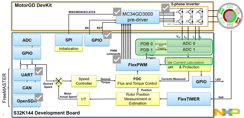 |
| Fig. 1: Application Mapping - HW & SW modules used for Phase Currents measurement are highlighted in green |
CURRENT SENSING METHODS
As designers or engineers in the field of power electronics, power supplies, battery management systems, motor drives and many other areas one of the most common faced problem is the need to measure currents accurately. In general the current needs to be measured for fault protection or functional control. For this application we need to measure the current for three main reasons:
- Functional - motor control feedback for FOC in order to orient the stator current vector
- Protection - against over-current and short circuit
- Information - about power consumption levels
In practice, there are four major current sensing methods commonly available. These methods are shown in table below, together with the advantages and disadvantages of each.
| Current Sensing Method | Construction | Advantages | Disadvantages |
|---|---|---|---|
Shunt Resistor | Low cost; Provides good accuracy; Wide-band measurements; |
High power dissipation; Not suitable for high current applications; | |
Conductor | Small or no-cost can be implemented directly on PCB tracks; Reduce BOM; | Poor accuracy due temperature variations; Need to be precisely calculated from beginning for proper balance between accuracy and power dissipation; | |
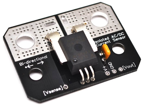
Hall effect sensor | Provides galvanic isolation; Low power dissipation; | High cost; Limited bandwidth; Needs additional electronic components; | |
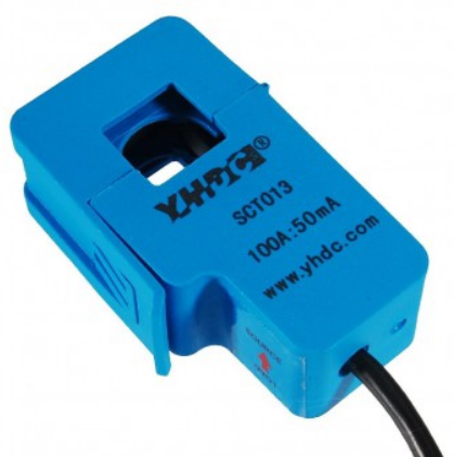
Current transformer | Provides galvanic isolation; High current sensing capabilities; | Large size & mass; Works only in AC; Requires special hardware to avoid magnetic saturation; Magnetic field susceptibility; |
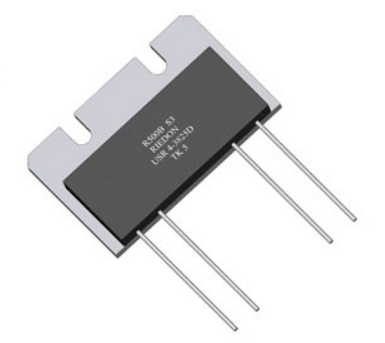
Based on the advantages of low cost and accurate wide-band measurement the precision shunt resistors, are frequently the best answer for most of the applications. In this case, choosing the best resistance R value is a question of balance between accuracy vs. power dissipation.
Shunt resistors works on a simple principle of Ohm Law: I = U/R. If the resistance R it is too high then power (P = I^2*R) will be wasted, excess heat will be generated and the voltage regulation is lost due to change in R value. Consequently, if R is too low then the sense voltage will be correspondingly low, so issues with noise and resolution will limit the accurate measurement of current.
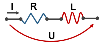
Another important aspect to consider when dealing with shunt resistors is the parasitic inductances that can cause wrong results. Any shunt resistor contains an inductance component that creates a voltage spike as shown in Fig. 2.
 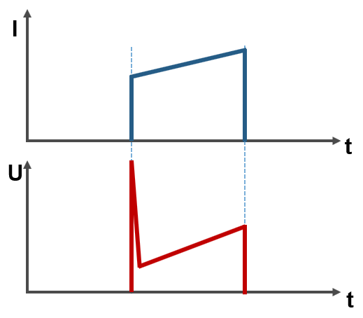 | |
| Fig. 2: Shunt parasitic inductance effect | |
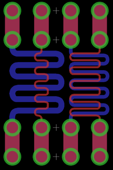
To reduce or eliminate the effect of parasitic inductances, special resistors and PCB layouts are used. The PCB track design around current shunt resistors is critical for obtaining an accurate current sensing. The main difference between dealing with a shunt resistor and a normal resistor is that four rather than two tracks must be provided to form a Kelvin connection, even where the component itself has only two terminals. These 2 additional tracks (V1-V2) that forms the Kelvin connection as shown in Fig. 3 are actually used for measuring the voltage drop across the shunt resistor, which is proportional with the current that needs to be measured.
The scope is to minimize the conductive path shared between the current path and the sensing loop, which would increase the tolerance on temperature variation and reduce the effect of parasitic inductance.
 | |
| Fig. 3: PCB design used to sense the currents via shunt resistors |
CURRENT MEASUREMENT STRATEGY WITH SHUNTS
Once the current sensing method is selected, the next step is to define how and where we are going to use the shunt resistors to acquire the information about the current. In motor control applications there are three main strategies that can be employed to accurately measure motor phase currents and the main difference between them is the relative position of the current sensors:
| Current Measurement Strategy | Sensor Type | Advantages | Disadvantages |
|---|---|---|---|
Inverter current sensing shunts (Dual-Shunt technique) | Less power dissipation since the current is not passing all the time thru it; Small shunt; Good balance between cost and PCB area; | Need 3 shunts resistors, one for each phase; Need to synchronize the readings with the times when lower switches are in conduction EMI noise due to proximity of inverter switches | |
DC-link current sensing shunt (Single-Shunt technique) | Single shunt needed; Small area footprint; BOM optimal | Large power dissipation capabilities Not suitable for high current applications Need complex SW to reconstruct the 3 phase currents | |
Motor phases current sensing shunts | Simplifies SW measuring routines since the current flow is continuously thru the shunt Can be swapped easily for supporting various current ranges | Very high power dissipation Large volume Additional PCB components needed to interface the sensors with the MCU logic |
The MotorGD DevKit comes equipped by default with all that is needed to address the first two use-cases as highlighted in Fig. 4:
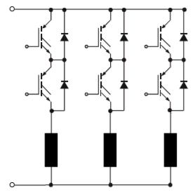
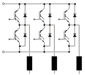
- Three inverter current sensing shunts, one for each inverter phase. Since in most of the cases the PMSM forms a 3-phase symmetric isolated system instead of sampling all three shunts resistors, you can use only 2 out of 3 to implement the standard PMSM phase current measurements which is also known as Dual-Shunt method. The third current can be easily computed in SW since Kirchhoff circuit law states that the sum off all 3 currents is null (Ia + Ib + Ic = 0)
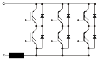
- One DC-link current sensing shunt that will be mainly used for current protection and power consumption monitoring. The current sensing information from this DC-link shunt can be used for what is called Single-Shunt method.
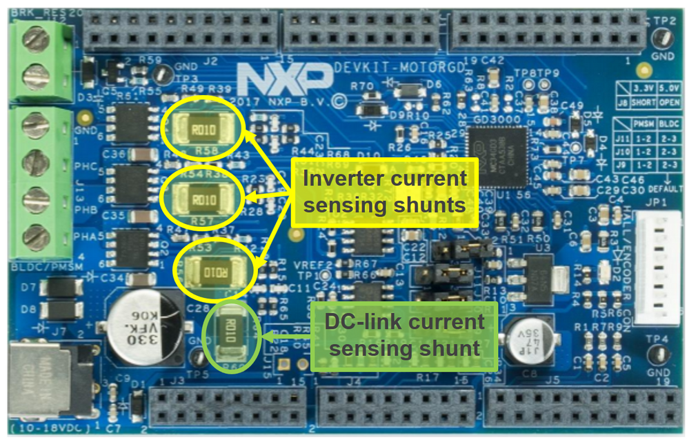 |
| Fig. 4: MotorGD DevKit Current measurement shunt resistors configuration |
DUAL-SHUNT SENSING TECHNIQUE
Dual-Shunt sensing techniques is one of the most common used method to measure the phase currents in motor control applications. This method have a good balance between advantages and disadvantages being suitable to be implemented in most of the applications. As depicted in Fig. 5, we are going to use the phase A and phase B inverter shunts to measure the voltage drop across the shunt resistor.
As it is depicted here and as mentioned before, the currents can be measured only when the lower switches are in conduction. Please notice i'm using the general naming convention as switch that incorporates a transistor and a anti-parallel diode. Depending on the load type and the commutation sequence the current may pass thru transistor or diode (for details about this please check: Module 4: Space Vector Modulation )
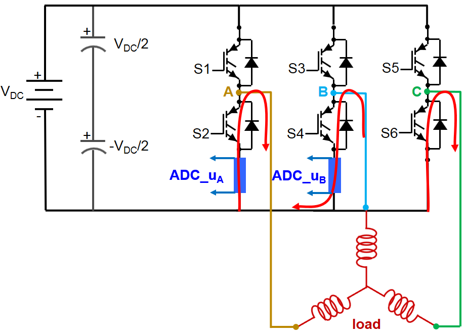 |
| Fig. 5: Dual-shunt current measurement topology |
As general assumption, the current that flows into the motor windings (as depicted in Fig. 5 by the current in phase A) will be considered as a positive current. Currents that flows out of the motor windings are considered to be negative current.
Since the shunt is placed in the lower part of the inverter, the voltage potential read from the shunt terminals is negative when the current flows into the motor winding. Therefore this need to be taken into consideration in SW when we are going to read the values from ADC. A negative voltage on the shunt resistor indicates a positive current thru the motor winding.
Another important aspect of dual-shunt measurement technique is PWM critical pulse width consideration. Since the ADC acquisition of the shunt voltage drop is done when the lower switch is activated, we need to maintain a minimal PWM command for that transistor in order to measure a relevant information.
This critical pulse width as depicted in Fig. 6, is needed for three main reasons:
- Voltage drop stabilization due to load inductance nature of motors. The effect of load inductance can be optimized but it can not be fully eliminated;
- System propagation delays between SW and HW components involved in the process. The delays form a chain that can be reduced by selecting components with fast response time but it can not be fully eliminated;
- ADC sampling and acquisition time can be optimized at design phase but never fully eliminated;
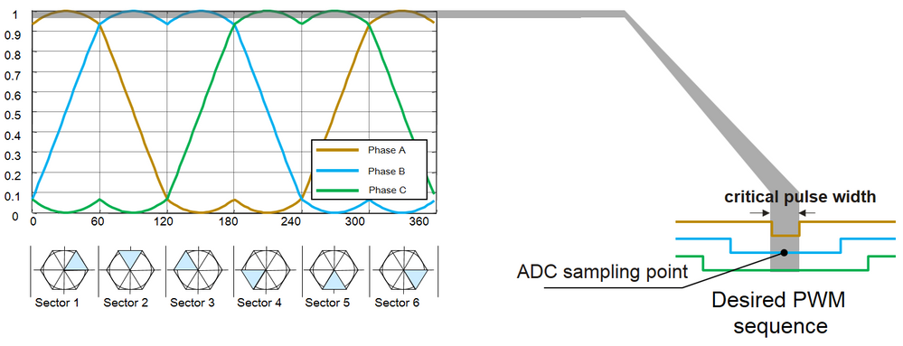 |
| Fig. 6: PWM critical pulse width in case of dual-shunt current measurement |
For a better understanding off all the variables we need to take into consideration lets us have a look at a typical shunt resistor voltage drop in case of a positive current passing thru. For readability, please consider the case of the phase A current measurement as depicted in Fig. 5.
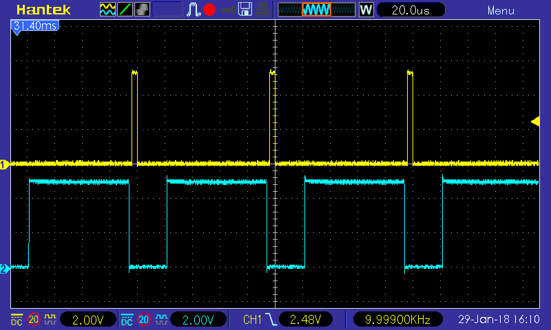
As it shown in this Fig. 7,oscilloscope capture using the MotorGD DevKit, with cyan we have the 10kHz PWM signal command that controls the lower inverter switch on phase A, while the yellow signal represents the voltage drop on the inverter phase A shunt resistor. When there is no current flowing thru the value of the drop voltage is zero. When the current flows thru the MOSFET the voltage drop as a stable value, while by the time the current flows thru the anti-parallel diode the voltage is slowly going down to zero.
For more details regarding the current flows thru transistor or diode please check the training video in Module 4: Space Vector Modulation
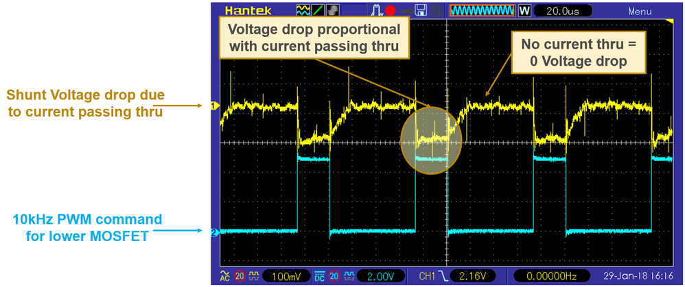 |
| Fig. 7: Voltage drop across a shunt resistor placed in lower part of inverter leg in case of the positive current passing thru |
If we zoom in a little bit we will see the effect of voltage drop stabilization time and why we need that delay when performing the current measurements. Any measurement in that region is prone to error due to current oscillations due inductance nature of the load. We have to wait until the current reaches a steady state regime thru the load and shunt before standing the ADC sampling and acquisition.
 |
| Fig. 8: Zoom in detail with shunt voltage drop stabilization. |
As it is shown in Fig. 7, in order to read the current you need to know then the lower switch is in conduction and more specifically when the current flows thru the MOSFET. Bottom line for an accurate current measurement, the ADC sampling must be synchronized with the PWM commands. To better understand this concept lets consider a simple inductor as load and lets assume we want to regulate the current thru such a load.
Fig. 9 shows the two possible scenarios that can be used for current measurement in this case and the effect of these tow scenario over the quantities acquired:
- In asynchronous sampling scenario, there is no correlation between the PWM signal (cyan waveform) and the ADC trigger (green waveform). The ADC conversion may happen to random time intervals as depicted in the upper case. Assuming the PWM duty factor is constant and the real current thru load varies in a saw-tooth waveform pattern, then the measured current will be wrong showing various levels depending on the moment the ADC was triggered.
- in the synchronized sampling scenario, the ADC conversion is triggered always in the middle of the PWM ON period. This mechanism will ensure that all the time we read the actual current thru the inductor in the same moment. The dark-red waveform shows that using this method we can read a steady average current all the time.
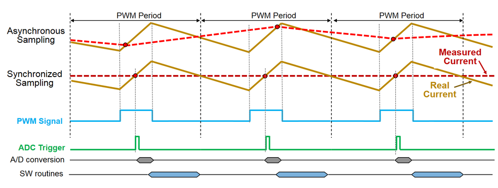 |
| Fig. 9: Asynchronous vs. Synchronous current measurement ADC sampling |
The last topic we have to discuss before implementing the actual application is the system delays that may affect the current measurements. Now that we know that we need to synchronize the PWM pulse generation with the ADC sampling we need to understand how various transformation between the moment when we compute the next PWM duty cycle until the moment we perform the measuring will affect the system. A typical processing chain is depicted in Fig. 10.
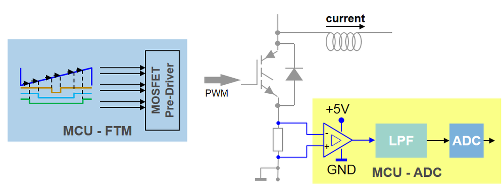 |
| Fig. 10: Processing chain between the MCU computation and actual current measurements |
Based on Fig. 10 system topology we can identify up to seven (yes! 7) sources of delays that add together and having a negative impact on the measurements. In the next table is shown the source of the delay, the overall impact and the typical numbers you should expect when dealing with such system topology as the one from MotorGD DevKit.
 |
Lets take it one by one and see how those delays influence the current measurements:
- PWM Dead time (DT) insertion. This is mostly given by the hardware design restrictions that needs to consider the type of load and the transistors used to switch the phase voltages. Since the transistors needs some time to enter or exit the conduction state, the SW must ensure there is no situation when both upper and lower transistors are in conduction at the same moment. A typical value for DT might be between 100ns up to 2us depending on various factors in the system. As shown in Fig. 11, after adding the dead time for on the desired PWM waveform, what we get is shift to the right for both PWM mid point and the rising edges. Therefore, immediately after finishing computing the proper PWM via Space Vector Modulation technique, we start to see the first delay.
 |
| Fig. 11: Delay due to Dead Time (DT) insertion |
- Between the moment when the PWM signal is computed and available inside the MCU FTM peripheral and the moment it reaches the actual MOSFET gate, there is an additional delaying chain cause by the signal response of various opto-couples and pre-drivers that are used to condition the signal and separates the high voltage side from low voltage one. This additional delay is shown in Fig. 12 and represent another shifting to the right of the PWM commands compared with the moment when FTM internal counter was initialized.
 |
| Fig. 12: Delay due to opto-coupler and pre-drivers |
- At this point in time the PWM command that controls the MOSFET transistor are available but all transistors have a time ON and OFF due to their intrinsic characteristics. Depending on the class of transistors you may have and the voltage level you need to switch ON/OFF, this delay may be shortef and longer. In Fig. 13, is show the entire delay (Delay2) between the theoretical switching point (marked here by the compare level CMP2) and the moment when the actual terminal voltage is switched.
 |
| Fig. 13: Delay due to transistors entering/exiting the conduction |
- Finally we reach to the point when the transistors are in conduction and the current have a path to flow thru the shunt resistor. In Fig. 14 is depicted the moment in time when the current start to flow. At this point you can see the delay between what has been commanded as what has been actually obtained as current flow thru motor winding.
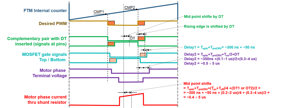 |
| Fig. 14: Delay between desired PWM command and the moment when current flows thru the shunt resistor |
- The last chain of delay that influence the current measurements is made of the low pass filter (LPF) shown in Fig. 10 and the amplifier slew rate as depicted in Fig. 15. As can be seen marked with a green circle the moment when the ADC can safety acquire the shunt voltage drop due to current passing thru is far to right delayed compared to the original desired PWM mid point.
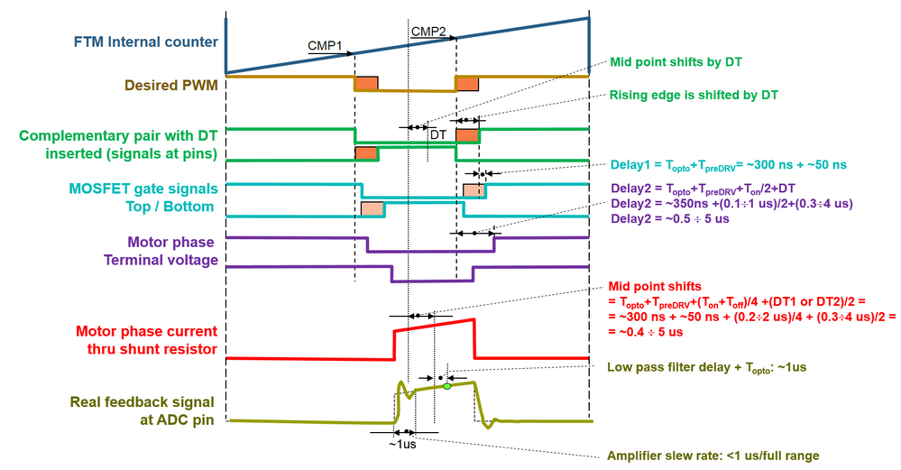 |
| Fig. 15: Delays due to filtering and amplifier slew rate |
Understanding and knowing all these factors will allow us to successfully read the correct values of the motor phase currents. As you can see, it is up to the software side to compensate for all these delays and perform the actual FOC accordingly.
HARDWARE SUPPORT
Now that we know what we have to do in order to read the currents, lets see that MotorGD DevKit is offerings and how can we use the signals to convert the information from analogue to digital. As shown in Fig. 16, we are going to use the inverter phase A and B shunts to capture the value of motor phase A and phase B. Based on these 2 values we are going to compute the third current on phase C.
 |
| Fig. 16: MotorGD DevKit 3-phase inverter schematic |
At this point you may ask yourself why not reading the phase C current directly since there is a shunt already available for that purpose. That is a legitimate question but due to the hardware constrains we are not going to use that third shunt and let me explain why.
As it has been explained the delays may have an big impact on the current measurements and this effect is even more important at high speed when we need to which the PWM faster. Spinning the motor faster it means we have to supply the motor with higher voltage that can only be achieved by maintaining the upper switches in conduction for longer time periods. In Fig. 6 was explained that we need a critical time interval to keep the lower transistor ON.
Therefore, considering the importance of reading the currents as closed as possible in the middle of the PWM lower switch command we would like to avoid doing multiple ADC sampling in that short time interval. The S32K144 MCU has two ADC modules and we can route the signals from both shunts to each of the ADC in order to sample in parallel the phase A and phase B currents. Any other combination will lead to an additional delay in measuring the phase C current and Kirchhoff law is going to be violated since the sampling is done to different moments in time.
Expect for the phase currents that needs to be sampled in the same time, nothing prevent us for measuring additional analogue values that does not need to be synchronized with the PWM waveform. As it shown in Fig. 17, we are going to read two additional signals that will helps us with motor and drive protection in the future. These two additional signals represent the DC-link voltage and current.
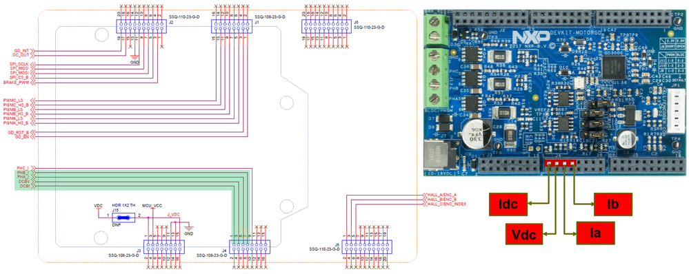 |
| Fig. 17: Analogue values to be read from MotorGD DevKit |
This signal are routed to the S32K144 MCU via dedicated pins that reach the ADC converters as shown in Fig. 18.
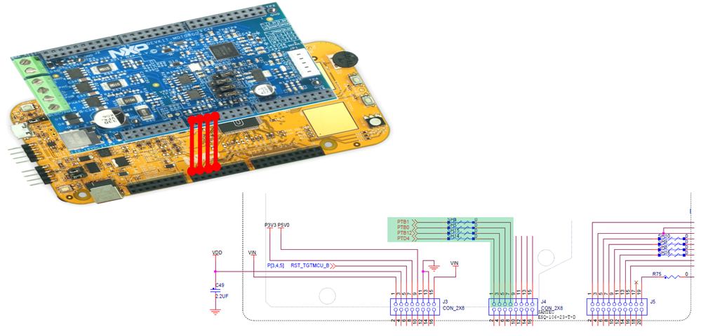 |
| Fig. 18: S32K144 analogue signal routing |
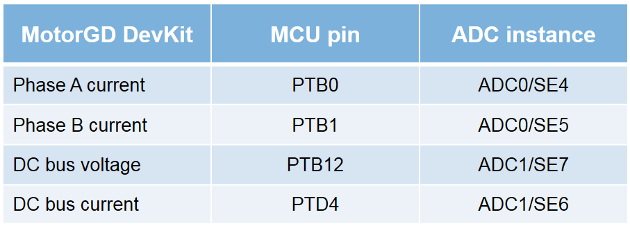
By default the correspondence between the signals and the ADC instances is shown in the table below. Note that the phase currents are routed by default to the same ADC0 converter. If we leave them like this is going to complicate the application since we will have to deal with an additional delay between the sampling moment of phase A current and the moment when we sample again to read the phase B current. In this time interval the current thru phase B might change the value and the FOC may be distorted.
 |
To solve these kind of issues, the S32K14x product families allows you to perform ADC hardware channels interleaving as shown in Fig. 19. In the hardware interleaved mode, a signal on the pin PTB1 can be sampled by both ADC0 and ADC1 in the same time. The interleaved mode is enabled by SIM_CHIPCTL[ADC_INTERLEAVE_EN] bits.
 |
| Fig. 19: S32K14x ADC hardware interleaved channels |
Using this hardware trick we are going to re-route the phase B current measurement to the ADC1 instead of ADC0 and the new analogue pin assignment will look like this:
 |
The last unknown piece of the puzzle is how synchronize the ADC measurement with the PWM command. Once again the S32K14x product family comes in handy with a rich feature set. The MCU contains a dedicated module for inter-connectivity of various hardware modules. This module is called TRGMUX and provides an extremely flexible mechanism for connecting various trigger sources to multiple pins/peripherals as shown in Fig. 20.
To trigger the ADC conversion we are going to use the FTM initialization trigger (INIT_TRIG) functionality. The INIT_TRIG is going to raise an event each time the PWM counter is re-initialized signaling this way the beginning of a new PWM period. This way the TRGMUX can re-route this event to the ADC modules to signal the moment when the ADC should start the acquisitions.
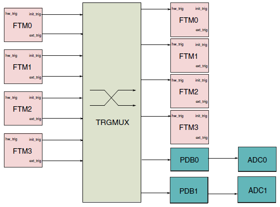 |
| Fig. 20: PWM - ADC synchronization |
As we have found out from Dual-Shunt Sensing Technique section, apart of PWM to ADC synchronization we also need to handle various sources of delays in the system. The S32K14x MCU families have a dedicated peripheral called Programmable Delay Block (PDB) that can trigger specific events based on a pre-condition.
In our case, we are going to configure the PDB instances to receive the same FTM INIT_TRIG event and to command the ADC acquisition at a specific moment in time which is delayed compared to the beginning of the PWM period. The specific delay timing intervals will be discussed in the next section.
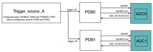 |
| Fig. 21: PDB triggering scheme of ADC conversion using same event synchronization source INIT_TRG |
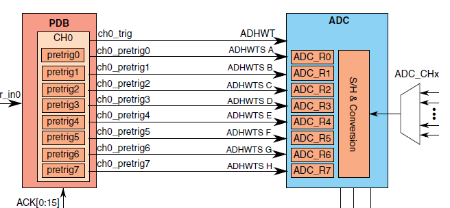
The overall ADC triggering concept can be summarize in Fig. 22. The FTM issue the counter initialization trigger which is used as a trigger input of the PDB. The PDB is then used to trigger the ADC. Each ADC channel in the PDB module supports up to 8 pre-triggers, which could be used as the ADC hardware channel selection to precondition the ADC block prior to an actual trigger. After a pre-trigger, the ADC trigger initiates the ADC conversion. When a PDB pre-trigger starts an ADC conversion, an internal lock associated with the corresponding pre-trigger is activated. This lock becomes inactive when receiving the conversion complete (COCO) signal from the ADC.
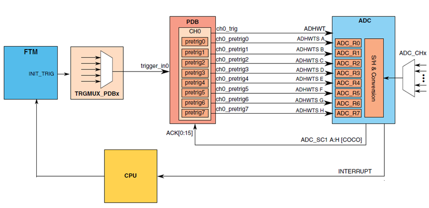 |
| Fig. 22: ADC trigger concept that implements the PWM-ADC synchronization |
As can be seen from Fig. 22 the main CPU is not involved in this mechanism once the entire chain of events is configured. This leaves more resources available for the programmer to implement the application.
EMBEDDED TARGET APPLICATION DEVELOPMENT
As mentioned in the Introduction, we are going to reuse and enhance the model developed in the previous module Module 5: V/F Scalar Control to perform:
- Hardware configuration for a proper current sensing using PWM-PDB-ADC synchronization
- Software computation for scaling the ADC conversion into the real values for currents and voltages
The Simulink blocks that are going to be added in this module are highlighted in Fig 23, in red while the blocks that are going to contain small modifications relative to the previous module are marked with magenta.
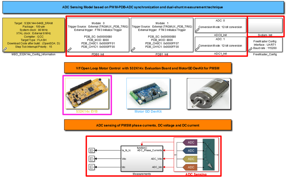 |
| Fig. 23: Top level Simulink model used for ADC measurements |
The Simulink model can be broken apart in various configuration steps as shown below.
MOSFET Pre-Driver Configuration
The first thing we have to do is to make sure MOSFET pre-driver is configured correctly according with MC34GD3000 datasheet. To do configure it correctly we need to perform a specific sequence of commands in order to make sure pre-driver outputs are enabled and latched prior to normal operation:
- RST input signal goes HIGH while the EN1 and EN2 input signals remain LOW;
EN1 and EN2 inputs are set to HIGH state
PA_LS_G, PB_LS_G, and PC_LS_G outputs are toggled HIGH for about 1.0 μs (HS outputs are enabled, but not latched)
Toggle PA_HS_G, PB_HS_G, and PC_HS_G outputs LOW for dead-time periord plus at least 0.1 μs
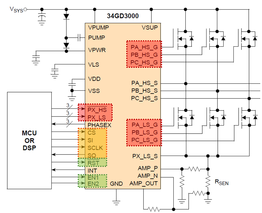 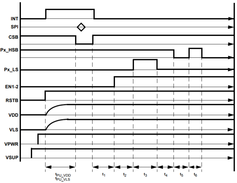 |
Fig. 24: MOSFET pre-driver configuration (a) - left side shows the pre-driver signals (b) - right shows the full initialization sequence |
The entire initialization sequence is implemented in Simulink using the State-Flow charts and triggered subsystems that mimics the sequence shown in Fig. 24b. The subsystem is implemented in the Fast Loop Control and it is executed only once after reset.
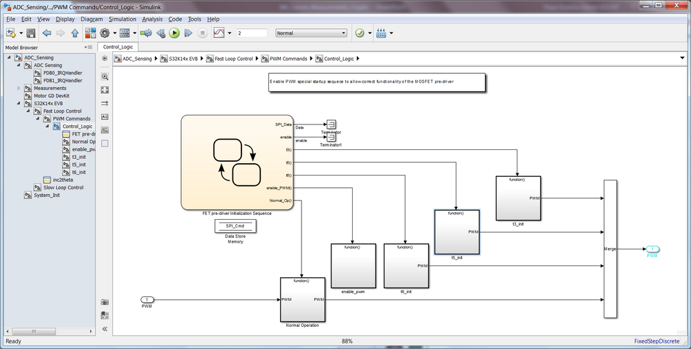 |
| Fig. 25: Pre-driver initialization Simulink model |
The SPI communication is not yet implemented since it is not in the purpose of this module. All the data are prepared and will be sent to the pre-driver in a future module when we will have to configure various hardware protections.
FTM Configuration
The Flex Timer Module needs to be configured to:
- perform a special PWM start-up sequence to enable the pre-driver configuration;
- send an interrupt each time the timer is getting reinitialized in order to allow PWM-PDB-ADC syncronization
Since we have to perform a special pre-driver configuration we need to make sure we have a full control over the moments when the PWM are activated. At initialization phase we are going to deactivate the PWM signal generation from "Start pin generation immediately after initialization" option and disabling "Initialization Trigger"
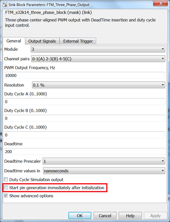 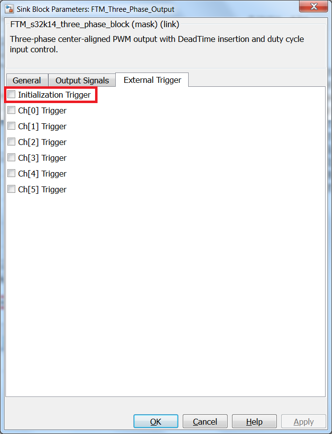 |
| Fig. 26: FTM_Three_Phase_Output Simulink block settings |
These two options will be enabled in the Control_Logic/enable_pwm subsystem shown in Fig. 25, where we have used an interesting combination of NXP Toolbox library blocks and Simulink Coder Custom Code blocks to call the FTM function that enables the trigger generation, as it is shown in Fig. 27.
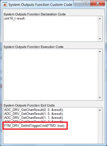 | ||
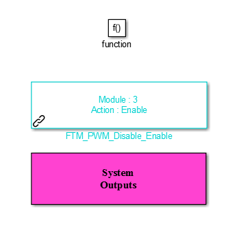
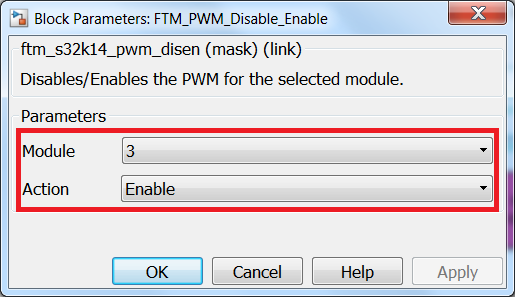
| Fig. 27: (a) pwm_enable subsystem, (b) FTM_PWM_Disable_Enable block configuration, (c) Simulink Coder Custom Code Block to call the function that setup the FTM initialization trigger | ||
ADC Configuration
First step in configuration of the ADC modules ADC0 and ADC1 is to configure the SIM module to interleave the ADC channels in order to allow us to read the phase current A and B in parallel on both ADC modules in the same time. Since there is no dedicated Simulink block for this we will have to write a custom piece of code that can be executed during system initialization phase. This is an easy task using the Simulink Coder dedicated blocks.
Using a Model Header Simulink Coder block we are going to write a generic function that could be reused to setup the SIM module that handles the ADC hardware channel interleaving. This piece of code is going to be place in the beginning of the C-file that is automatically generated by Simulink for our model.
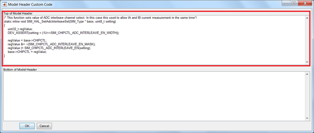 |
| Fig. 28: SIM model interleave function body |
All that remains now is to call this function at the initialization stage with the proper arguments that configures the PTB1 input to be sampled by the ADC1 on AD15 input channel.
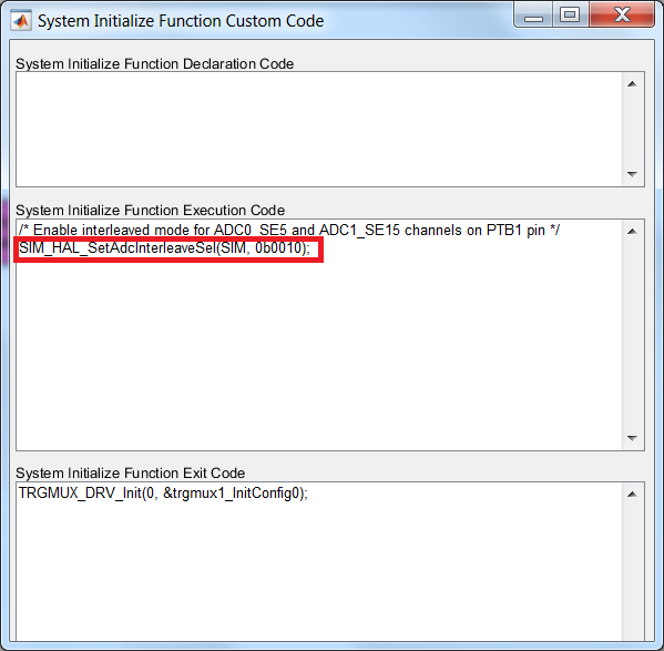 |
| Fig. 29: ADC interleave selection for PTB1 input |
The initialization for both ADC modules ADC0 and ADC1 is identical. The main parameters that needs to be configured are shown in Fig. 30. For more details of each one please consult the Help. As shown here, the ADC are configured to use the highest resolution possible and to have the conversions automatically started based on hardware event controlled by the PDB peripheral
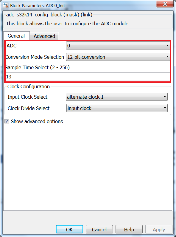 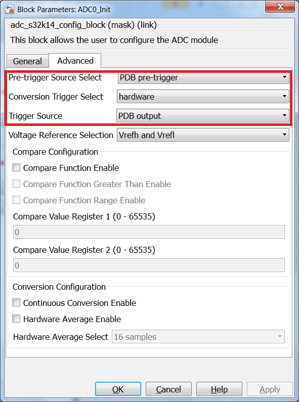 |
| Fig. 30: ADC instances configuration |
The final ADC configuration that needs to be done is to setup the conversion channels associated with the values we want to measure. The ADC conversion results are currently read in the PDB interrupt handle which is synchronized with the FTM PWM initialization trigger.
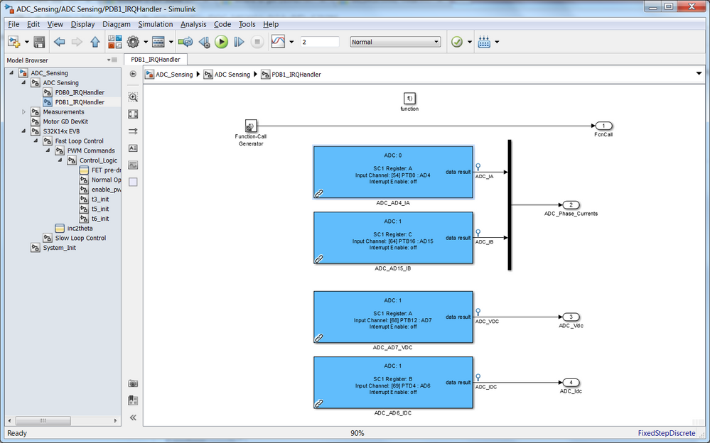 |
| Fig. 31: Simulink model for ADC conversion results reading |
The second part of this article can be found here: https://community.nxp.com/thread/469526
- Mark as New
- Bookmark
- Subscribe
- Mute
- Subscribe to RSS Feed
- Permalink
- Report Inappropriate Content
Hello dumitru-daniel.popa
I couldn't find the page you posted...
Page Not Found
The page you requested cannot be found.
Possible reasons for missing pages, and what you can do:
- If you typed a URL in the Address bar, make sure the URL was spelled correctly.
- If you used a bookmark, please delete it and navigate from the homepage.
- If you cannot find a product or page and need technical assistance, please enter a service request.
- This page may not be available in the language you selected
- Mark as New
- Bookmark
- Subscribe
- Mute
- Subscribe to RSS Feed
- Permalink
- Report Inappropriate Content
- Mark as New
- Bookmark
- Subscribe
- Mute
- Subscribe to RSS Feed
- Permalink
- Report Inappropriate Content
of course I have some further questions with configuring the PDB/ADC/FTM.
I will try to do this step by step...
1) Your "FTM_Three_Phase_Output" is Module 3, why you have Chosen "FTM2 External Trigger" in your PDB0 and PDB1 init blocks ?
2) I understand that you Trigger the ADC samples at different timing Points of one PWM cycle. For that you use the pre-Trigger Option in the PDB blocks. Your ADC sensing is done in a PDB_ISR. How do you know which ADC sample is done with which pre-trigger ?
It should be:
PDB0 - Delay6900 - Pre-trigger0 --> ADC0, Ia (Interleaving activated)
PDB1 - Delay0 - Pre-trigger0 --> ADC1 Vdc
PDB1 - Delay4100 - Pre-trigger1 --> ADC1, Idc
PDB1 - Delay6900 - Pre-trigger2 --> ADC1, Ib
3) For the delays you set this:
Ia, Ib --> 6900/8000 = 86,25us
Idc --> 4100/8000 = 51,25us - In your Fig. 35 you pointed at the Peak of dc link current, which is at 70us ??
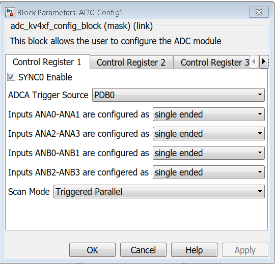
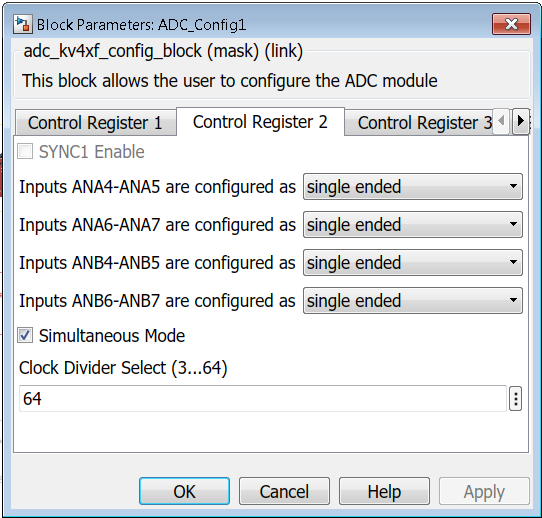
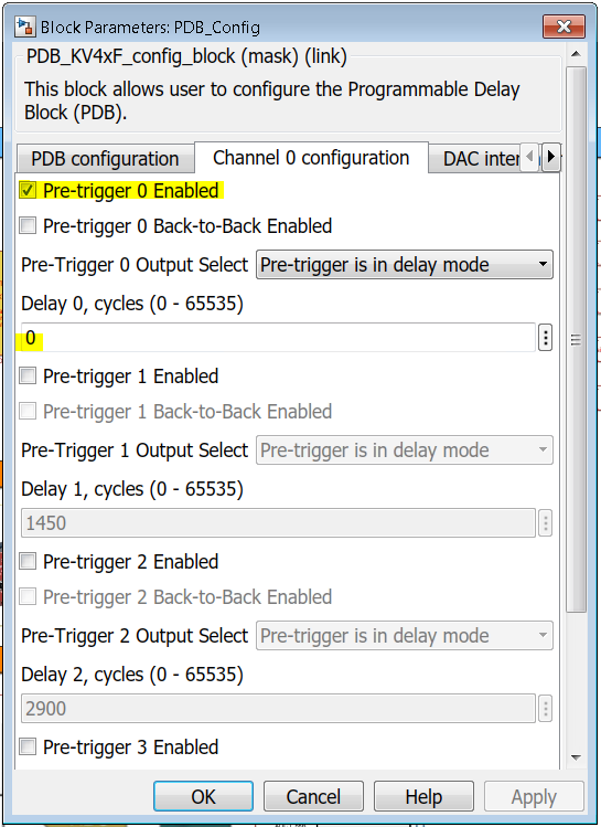
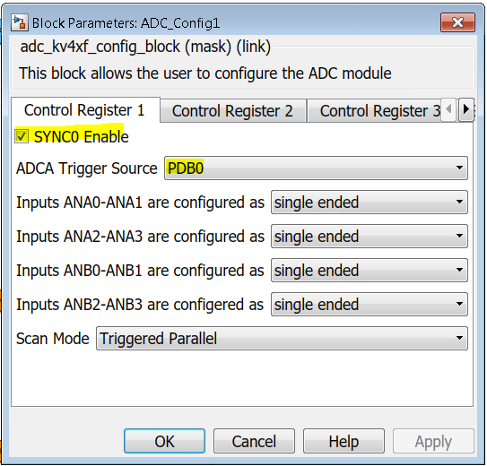
4) With KV4x the adc configuration block is a Little bit different. I have configured this to trigger the adc via PDB and use the simultaneous mode. Because of the simultaneous mode I think that I only Need the PDB0 which then will Trigger ADC0 and ADC1 together at the same time ?
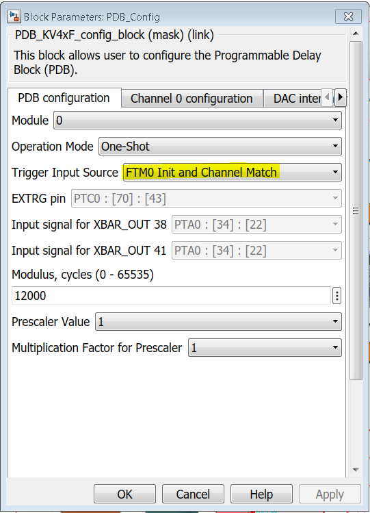
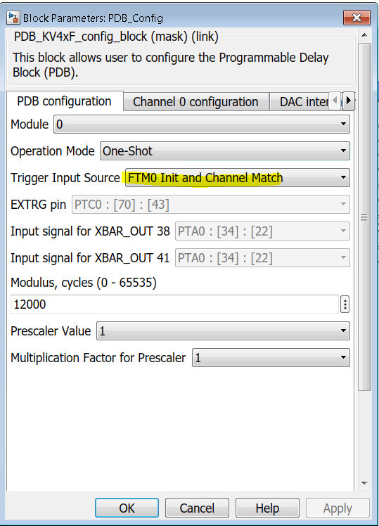
I use the "FTM_Three_Phase_Output" Module 0, so I have set "FTM0 Init and Channel Match" in the PDB_Config. Is that correct ?
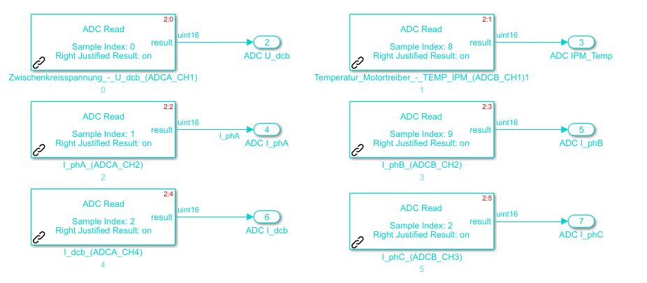
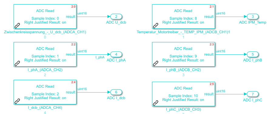
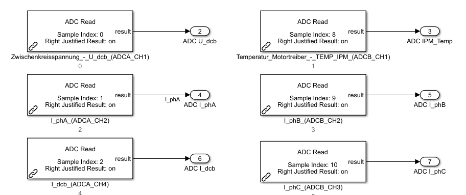
The PDB0-interrupt handler subsystem should then contain all the ADC Read blocks for ADCA and ADCB ? You can see themin the Image below:
Here is the same question like above: How do I know at which timing the ADC is read ?
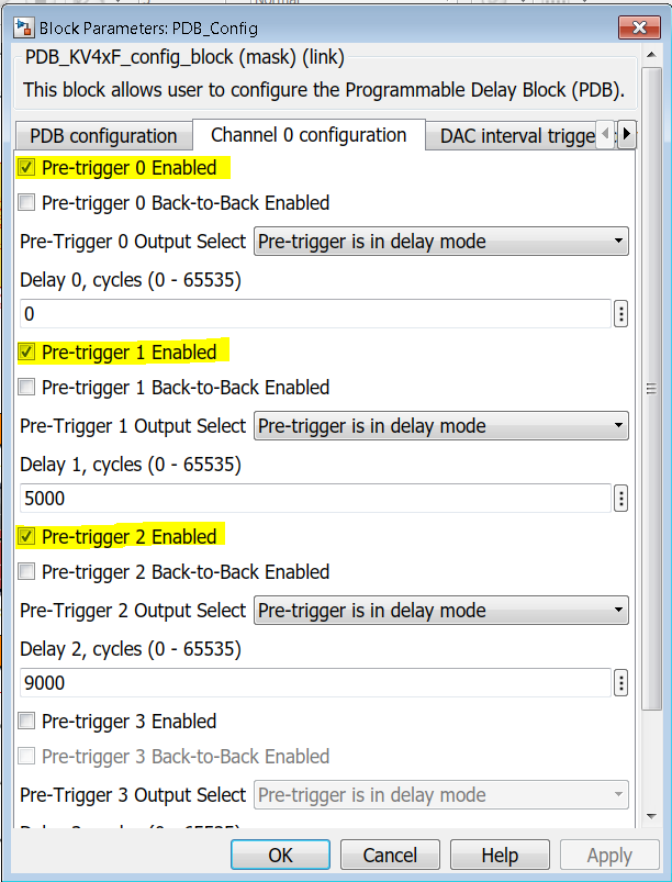
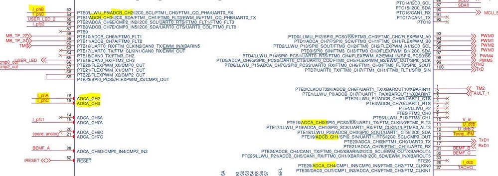
In case of KV4x PDB config, It is only possible to configure 4 pre trigger. So I have to use 3 of them at the Moment because I have 6 measurements (U_dcb, I_phA, I_dcb, Temp_IPM, I_phB, I_phC):
Is that an accurate way or should I better deactivate the simultaneous mode in adc config, then trigger ADC0 with PDB0 and ADC1 with PDB1 (PDB config would be the same for both - FTM0 as trigger source like shown above) and use two PDB_interrupt handler Subsystems ? Each of them would contain three ADC Read blocks.
I understand that It would be better to calculate I_phC in Software. Anyway I Need 5 measurements in my case (U_dcb, I_phA, I_dcb, Temp_IPM, I_phB), so 3 samples are needed.
Any recommendation to improve this ?
Kind regards
Leon
- Mark as New
- Bookmark
- Subscribe
- Mute
- Subscribe to RSS Feed
- Permalink
- Report Inappropriate Content
Hi Leon,
1) Your "FTM_Three_Phase_Output" is Module 3, why you have Chosen "FTM2 External Trigger" in your PDB0 and PDB1 init blocks ?
Nope, i've selected the FTM3 Initialization trigger. You can see that selection in
Fig. 37: PDB0 and PDB1 global configurations: trigger source, external trigger type and PDB counter value within Module 6: Current Sensing (Part 2/2)
Also, 
Your ADC sensing is done in a PDB_ISR. How do you know which ADC sample is done with which pre-trigger ?
There is a specific HW arrangement that "connects" each PDB pre-trigger to each ADC hardware channel.
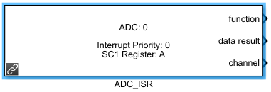
The actual pre-trigger vs. ADC channel pairing is done via SC1 Register selection. If you wish to have a particular order in which you capture the analogue conversions then you simply assign the appropiate latter A, B, C, D, etc to the conversion block: A corresponds to R0, B to R2 and so on.
Idc --> 4100/8000 = 51,25us - In your Fig. 35 you pointed at the Peak of dc link current, which is at 70us ??
You do not need the peak value - but rather the average since we are dealing with very short bursts due to PWM.
Regarding the KV4x specifics i'm not 100% aware off since i've not practice using it. As far as i remember there was an older thread you have opened in which you managed to measure the currents.
How do I know at which timing the ADC is read ?
I used an oscilloscope to verify when the last ADC conversion happens. For that i've activated the ADC ISR for that particular conversion and i toggled a GPO in that ISR handler - in my case the IB current. Then I've checked that GPO against the actual PWM Low Signal.
Anyhow - in case the timings are not correct you will get PDB errors.
understood that It would be better to calculate I_phC in Software. How I have to configure the adc to make 5 instead of 6 measurements (ADCA: U_dcb, I_phA, I_dcb - ADCB: Temp_IPM, I_phB) ?
Yes, it is better to read just 2 currents because due to conversion delay you might end up with ia+ib+ic != 0
Best regards,
Daniel
- Mark as New
- Bookmark
- Subscribe
- Mute
- Subscribe to RSS Feed
- Permalink
- Report Inappropriate Content
Hi Daniel,
again a Long post, but I think with important Content to understand the PWM, ADC Trigger Timing.
Perhaps something went wrong during import of the slx in your Environment.
Only for your info. I downloaded the example again and if I open it then there is "FTM2 External Trigger" configured.
I do not have the "FTM3 Initialize Trigger" Option, only "FTM3 Internal Trigger" or "FTM3 External Trigger" for S32K.
I think "FTM3 Internal Trigger" would be the same like "FTM3 Initialize Trigger" ?
Maybe this is because you saved the model in 2015b ?
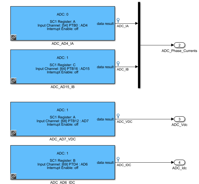
The actual pre-trigger vs. ADC channel pairing is done via SC1 Register selection. If you wish to have a particular order in which you capture the analogue conversions then you simply assign the appropiate latter A, B, C, D, etc to the conversion block: A corresponds to R0, B to R2 and so on.
Ok I think I understand, your PDB1_IRQHandler:
ADC0, Pre-trigger0 - SCI Register A - Ia (6900 cycles)
ADC1, Pre-trigger0 - SCI Register A - Vdc (0 cycles)
ADC1, Pre-trigger1 - SCI Register B - Idc (4100 cycles)
ADC1, Pre-trigger2 - SCI Register C - Ib (6900 cycles)
Now KV4x
With KV4x It is only possible to configure the sample indes and I don't have this SCI Register Options like you see here:
Also in the ADC Sample or ADC Config block I didn't found this SCI Option. So how do I know which ADC pair is read with which pre-trigger here?
Actual I use one PDB_config (module 0) and adc works in simultaneous mode. So I would expect this:
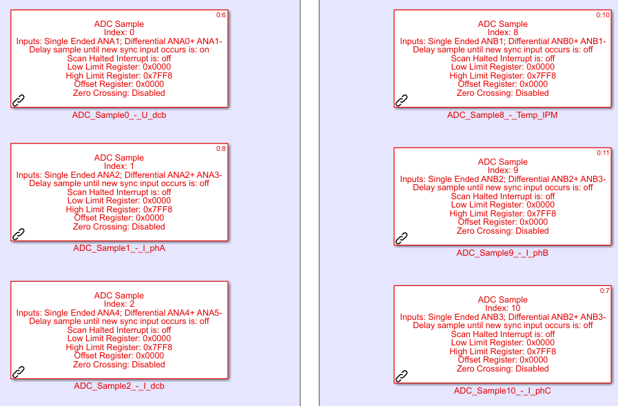
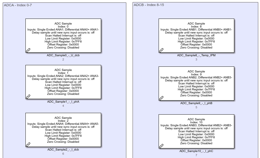
Pre-trigger0 - ADCA Sample Index 0, ADCB Sample Index 8
Pre-trigger1- ADCA Sample Index 1, ADCB Sample Index 9
Pre-trigger2 - ADCA Sample Index 2, ADCB Sample Index 10
Is that correct or am I wrong ? I also have looked in the KV4x Reference Manual, but it is not specially announced here which pre-trigger is for which adc sample.
The PDB config:
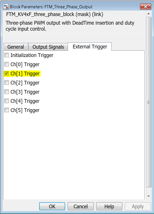
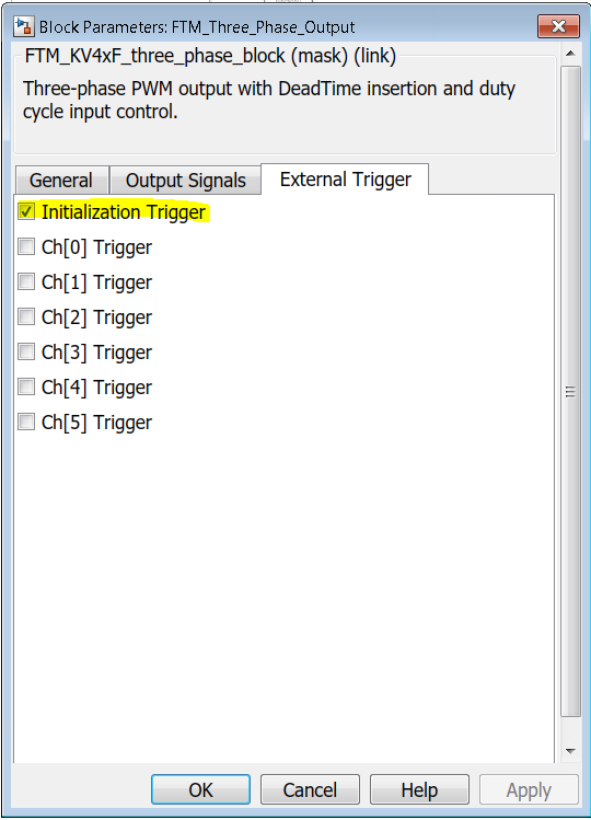
The PDB_Interrupt only works if I activate the external Trigger Option in the FTM_Three_phase_Output block. Ch[1] Trigger should be the Moment of the LowSide IGBT A is in conduction ? This would be valid for I_phA but not for I_phB and I_phC ? Or should I configure "Initialization Trigger" ?
You don't have activated this Option in your s32k model...? But maybe because you was able to choose "FTM3 Initialize Trigger" in the PDB config ?
Obviously I don't exactly understand the Connection between "External Trigger" in FTM_Three_Phase_Output, PDB Trigger Input Source "FTM0 Init and Channel Match", PDB Pre-trigger 0,1,2 and ADC Sample. Could you explain that for me for KV4 ?
I used an oscilloscope to verify when the last ADC conversion happens. For that i've activated the ADC ISR for that particular conversion and i toggled a GPO in that ISR handler - in my case the IB current. Then I've checked that GPO against the actual PWM Low Signal.
In your case with s32k you might use this one so you could configure a specific ADC and SC1 Register. So you could see the exact time of the adc conversation you want to see.
In Kv4 Toolbox I found this, so I could only see the end of scan is complete. I do not exactly know which ADC Sample pair (in simultaneous mode) was read.
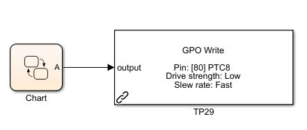
I checked this with a testpin and it changes the state three times in one pwm cycle period.
Also I'm able to manipulate the time of switching the state with the pre Trigger value.
Still the question which pre-trigger is connected to which adc sample pair. (see above)
Yes, it is better to read just 2 currents because due to conversion delay you might end up with ia+ib+ic != 0
I understand that It would be better to calculate I_phC in Software. Anyway I Need 5 measurements in my case (U_dcb, I_phA, I_dcb, Temp_IPM, I_phB), so 3 samples are needed in simultaneous mode.
Any recommendation to improve this or would a reduction of 1 sample necessary lead to give up one additional measurement (e.g. IPM Temp).
Kind regards
Leon
- Mark as New
- Bookmark
- Subscribe
- Mute
- Subscribe to RSS Feed
- Permalink
- Report Inappropriate Content
Hi Leon,
I think i know what's going on. During the workshop development i found an issue with FTM initialization triggers. To fix that you will need S32K1xx v3.0.0 and the software path: https://community.nxp.com/thread/467438
After that you should be able to see it.
mariuslucianandrei can you have a look over the ADC settings for Kinetics. I know you have done some investigation in the past.
Best regards,
Daniel
- Mark as New
- Bookmark
- Subscribe
- Mute
- Subscribe to RSS Feed
- Permalink
- Report Inappropriate Content
Hi Daniel,
you are right !
With the Hotfix I'm now I am able to choose "FTM3 Initial Trigger" Option with S32k
What I have to choose in the external Trigger tab with kv4 ?
Best regards
Leon
- Mark as New
- Bookmark
- Subscribe
- Mute
- Subscribe to RSS Feed
- Permalink
- Report Inappropriate Content
Hello dumitru-daniel.popa
I think I have made it with KV4, so I want to Show it here !
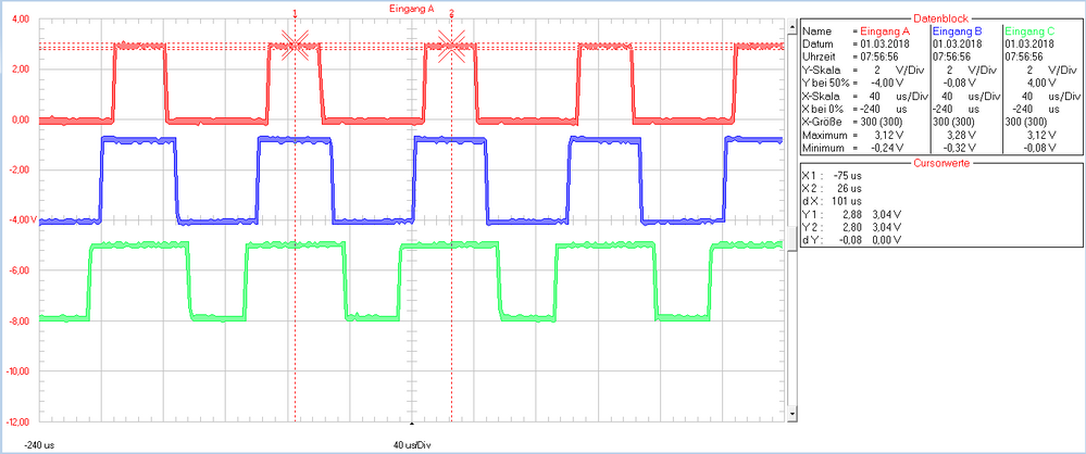
First of all the three PWM low side igbt signals:
Now I have set the Initialization Trigger in the external Trigger tab of "FTM Three Phase Output", which should be exactly in the middle of PWM low side Signal.
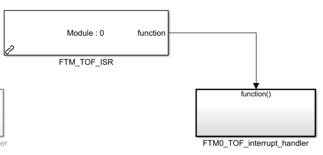
With the Timer Overflow I checked the time of the initialization with a testpin
TOF Interrupt handler:
In the PDB config block I have configured "FTM0 Init and Channel Match"
I only configured one Pre-Trigger in the Channel 0 configuration without any delay.
The ADC(in simultaneous mode) is triggered from the PDB0
The configured ADC samples:
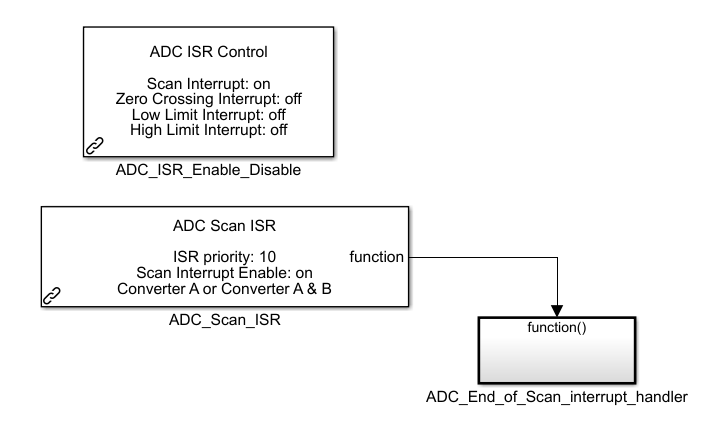
After the PDB triggeres the ADC all ADC samples are read !
After the end of scan I checked this with a second testpin
End of Scan Interrupt handler
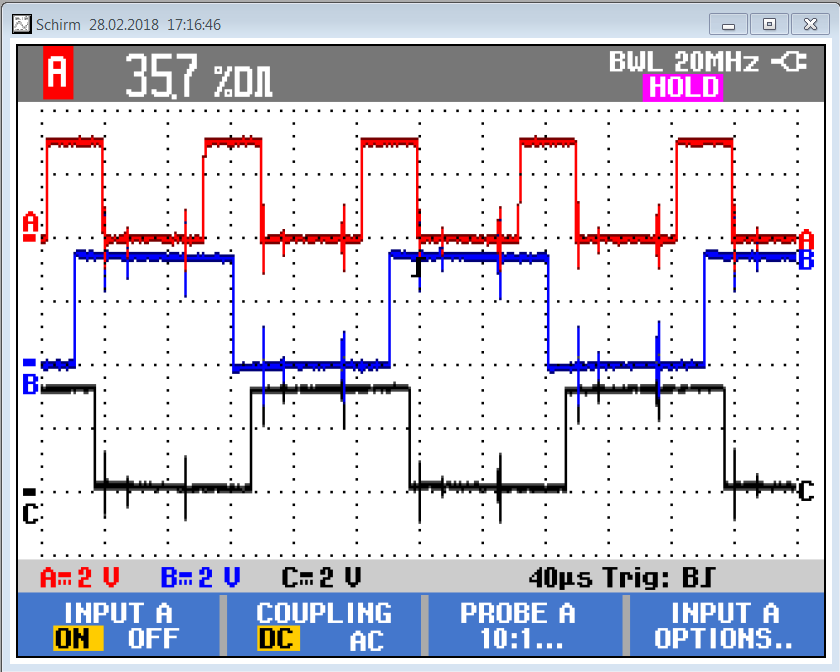
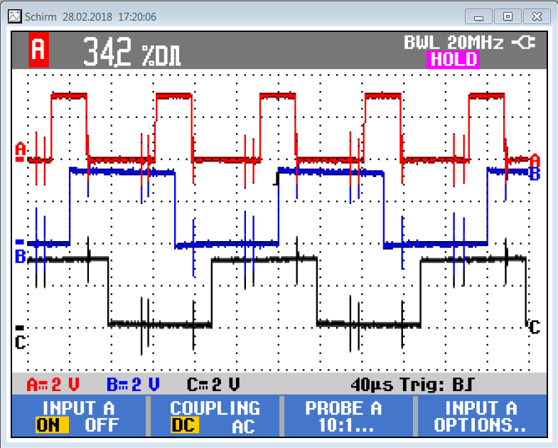
Here you can see the PWM A low side (red) Timer Overflow (blue) and ADC End of Scan (black) with pre Trigger delay 0
The same with pre-Trigger 3000, you see the time of switching the state of the black Signal is later (this would lead to Problems because the low side IGBT isn't in conduction over the complete measurement.
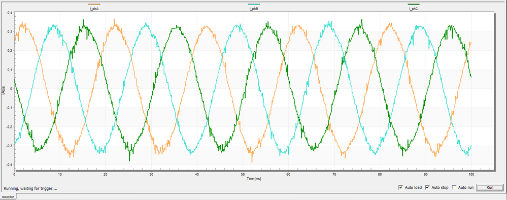
The currents in freemaster:
Now let me ask something.
Obviously all the configured ADC samples are read if the pdb triggeres the adc in the middle of pwm low side Signal.
So also U_dcb, IPM_Temp and I dcb are read here, which requires sample time.
To improve the measurement it would be better only to measure I_phA and I_phB directly with the Initialization Trigger.
The measurement of the other samples U_dcb, IPM_Temp could be leter in the pwm cycle
Do you know a way for this, so to seperate the Timing of reading the different samples ?
I'm not quite sure with I_dcb, at which Point of one PWM cycle this should be read ?
Best regards
Leon
- Mark as New
- Bookmark
- Subscribe
- Mute
- Subscribe to RSS Feed
- Permalink
- Report Inappropriate Content
Hi Leon,
Congrats!!! You current measurements looks very good/clean. In my case i had to deal with various sources of measurements noise - but in your case i see the results are quite perfect.
Do you know a way for this, so to separate the Timing of reading the different samples ?
Yes, you can do that.
I'm not quite sure with I_dcb, at which Point of one PWM cycle this should be read ?
There is no bullet prof method. As for the currents you need to perform some tests to see where you can read the correct values. In general the ADC reads are quite fast so you should have plenty of time to complete the acquisition.
In my case on S32K i had to choose the delay by comparing the ADC acquisitions against the DC current read with an AmpMeter in series with the source.
I think it would be a good idea to present your work in a separated thread once you have completed the model. We encourage everyone to do so and if you think it is appropriate you could also share your final model in that thread - its up to your if you want to give it for free or not - but i think is a good opportunity to promote your work in this space.
Best regards,
Daniel
- Mark as New
- Bookmark
- Subscribe
- Mute
- Subscribe to RSS Feed
- Permalink
- Report Inappropriate Content
Hi Daniel,
Do you know a way for this, so to separate the Timing of reading the different samples ?
Yes, you can do that.
Maybe you could show me how to do that with KV4 ?
With an additional pre-Trigger the End of Scan Interrupt occures two times, so with every pre Trigger all samples are read in the Moment. This might be worse for I dcb, because it would also be read while the pwm low side igbt is in conduction. I did not check the correct moment for this measurement quite now.
In my case on S32K i had to choose the delay by comparing the ADC acquisitions against the DC current read with an AmpMeter in series with the source
Okay thank you for this ! If I would be able to seperate the samples I could configure a different Moment for the I dcb sample.
Best regards
Leon
- Mark as New
- Bookmark
- Subscribe
- Mute
- Subscribe to RSS Feed
- Permalink
- Report Inappropriate Content
Next question...
I found that you now used "Periodic Interrupt Timer" instead of "Function Call Generator" with specified Sample Time S_LST = 1ms and C_LST = 0.1ms to call the Slow and Fast Loop Subsystems.
Am I right that this was done because the PIT is synchronized with PWM Timing ?
Function Call Generator block is periodic but not necessarily synchronized with the PWM ?
With KV4x there also isn't the "Start Counter immediately after initialization" Option in the PIT block like I mentioned before with the "eFlexPWM_Three_Phase_Output" and "FTM_Three_Phase_Output".
Does this make any Problems ?
Also the ISR priorities are not clear for me.
PIT Channel 1 - priority 4 (Fast Loop)
PIT Channel 2 - priority 4 (Slow Loop)
PDB1 - priority 1 (Module 1)
PDB0 - priority 10 (Module 0)
- Mark as New
- Bookmark
- Subscribe
- Mute
- Subscribe to RSS Feed
- Permalink
- Report Inappropriate Content
Hi Leon,
Indeed, I switched to PIT timers in preparation for the next modules (M7-M10) that will use the function calls. The original function call was used only in M5 as a way to have a comparison between the Simulation vs. Hardware since for simulation i can't use PIT block.
The generated code for the function call is a bit ugly and that is why i preferred to switch to PIT - timer interrupts since it is easy to read the code.
Anyhow, there is no issue with the synchronization since Simulink Step Function where all the computation are updated is in sync with the rest of the clocks PWM/ADC/PIT. It is the same clock source used.
With KV4x there also isn't the "Start Counter immediately after initialization" Option in the PIT block like I mentioned before with the "eFlexPWM_Three_Phase_Output" and "FTM_Three_Phase_Output".
Does this make any Problems ?
It should not be. As i explained before - i was bounded to the HW implementation and the initialization of the MC34GD pre-driver. I could probably move that all together in the Simulink Initialization Function but one of the reasons behind these training is to advertise different functionalities the toolbox is capable off.
Also the ISR priorities are not clear for me.
PIT Channel 1 - priority 4 (Fast Loop)
PIT Channel 2 - priority 4 (Slow Loop)
PDB1 - priority 1 (Module 1)
PDB0 - priority 10 (Module 0)
Thank for highlighting this. It's my fault. it should be: PDB1, PIT1, PIT2, PDB0 priority order.
Best regards,
Daniel
- Mark as New
- Bookmark
- Subscribe
- Mute
- Subscribe to RSS Feed
- Permalink
- Report Inappropriate Content
Hello dumitru-daniel.popa,
first thank you again for this module which is really important to implement the FOR later on.
I think with the KV4x it will be a little bit different to trigger the ADC with the PWM.
The currents are already matched to the two ADC modules, so no interleaving should be required ?
Also the initialisation routine could not be the same, because there is no "PWM Enable/Disable" block in the KV4x library? The "Start pin generation immediately after initialization" option I couldn't found in the "FTM_Three_Phase_Output" or "eFlexPWM_Three_Phase_Output". What I have to consider here ?
If I use the "FTM_Three_Phase_Output" I principle could use your way with Simulink Coder Custom Code blocks to call the FTM function that enables the trigger generation ?
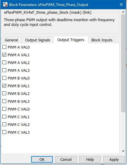
With the "eFlexPWM_Three_Phase_Output" I could use the Output trigger tab shown below ?
Also I have a simple question to the beginning:
Why you set 8000 cycles in the PDB configuration ? I think this corresponds to 10kHz ? But why ?
Best regards
Leon
- Mark as New
- Bookmark
- Subscribe
- Mute
- Subscribe to RSS Feed
- Permalink
- Report Inappropriate Content
Hi Leon,
think with the KV4x it will be a little bit different to trigger the ADC with the PWM.
The currents are already matched to the two ADC modules, so no interleaving should be required ?
Indeed, no interleave required in your case.In case of S32K14x and MotorGD that needs to be done since that is how the hardware was designed. In case of custom design - knowing that MCU support interleaving might save you from a lot of troubles regarding pin assignment and signal routing.
Also the initialisation routine could not be the same, because there is no "PWM Enable/Disable" block in the KV4x library? The "Start pin generation immediately after initialization" option I couldn't found in the "FTM_Three_Phase_Output" or "eFlexPWM_Three_Phase_Output". What I have to consider here ?
Yes, some of the older toolboxes does not have such options. In case of KV the PWM signal generation are done at the initialization stage.
That should not pose any important issues. Still make sure that at the startup the commands that are passed to the PWM are initialized with a same value that does not create a voltage potential at motor terminals. A good practice is to make sure at initialization the default duty cycle is 50% or the high and low signal are not overlapping.
Also, make sure the PWM block has the lowest priority in the model compared with the initialization of the other block like ADC, timers, etc.
Depending on the relative Simulink priority, the PWM should be the last block to be configured in Simulink initialization phase. This way to make sure that all the other blocks that depends on the PWM are not started accidentally.
If I use the "FTM_Three_Phase_Output" I principle could use your way with Simulink Coder Custom Code blocks to call the FTM function that enables the trigger generation ?
That's a bug in our current toolbox for S32K - we can enable the trigger only once and since i need the special initialization sequence of the MC34GD3000 predriver i was forced to re-enable the trigger. I used the custom code to workaround that issue :-)
You do not need it.
With the "eFlexPWM_Three_Phase_Output" I could use the Output trigger tab shown below ?
Yes!
Why you set 8000 cycles in the PDB configuration ? I think this corresponds to 10kHz ? But why ?
The S32K14x operates at 80MHz. To obtain a 10kHz frequency from the PWM you need a counter that counts up to 80MHz/10KHz = 8000 ticks.
The PDB is syncronized with PWM, therefore the PDB counter is also set to restart at 8000 counts.
Best regards,
Daniel
- Mark as New
- Bookmark
- Subscribe
- Mute
- Subscribe to RSS Feed
- Permalink
- Report Inappropriate Content
thank a lot for your remarks ! Let me ask some things to become clearer.
Still make sure that at the startup the commands that are passed to the PWM are initialized with a same value that does not create a voltage potential at motor terminals. A good practice is to make sure at initialization the default duty cycle is 50% or the high and low signal are not overlapping.
So the only thing to do in this case is to configure the "Initial Duty Cycle A", "...B", "...C" in the "eFlexPWM_Three_Phase_Output" or "FTM_Three_Phase_Output" ?
At the Moment I have set 0%, so only the low side IGBT are in conduction and the terminals are connected to ground.
Is that a good way or should I set 50% instead of 0% Initial duty cycle ?
Also, make sure the PWM block has the lowest priority in the model compared with the initialization of the other block like ADC, timers, etc.
Depending on the relative Simulink priority, the PWM should be the last block to be configured in Simulink initialization phase. This way to make sure that all the other blocks that depends on the PWM are not started accidentally.
The only way I know is to set priorities in the block properties ? With this it is possible to Change the execution order.
Is this the way you suggest ? Or is there another way to influence the initialization phase ?
we can enable the trigger only once and since i need the special initialization sequence of the MC34GD3000 predriver i was forced to re-enable the trigger. I used the custom code to workaround that issue :-)
You do not need it.
The KV4x "FTM_Three_Phase_Output" has no "Output Trigger" tab like "eFlexPWM_Three_Phase_Output".
How could I generate a trigger with FTM_Three_Phase_Output every PWM sequence with KV4x?
S32K Toolbox has no "eFlexPWM_Three_Phase_Output", so for working with KV4x I should simply use this to use the Trigger event ?
Best regards
Leon
- Mark as New
- Bookmark
- Subscribe
- Mute
- Subscribe to RSS Feed
- Permalink
- Report Inappropriate Content
Hello Daniel,
with FTM_CHN_ISR block I'm now able to generate a Trigger Event at the Moment the lower IGBT is in conduction.
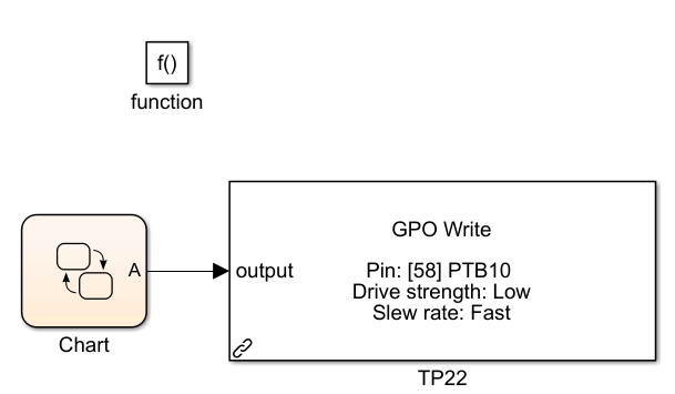
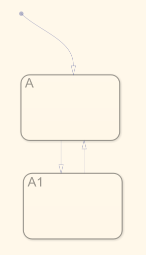
but with the stateflow diagram below of course the pin only switches every time the trigger occurs.
Could you Show me your example to Switch back the testpin before a new Trigger Input occurs ?
with eFlexPWM_Interrupt I get this message...
It is just copied out of the "kv4xf_eflexpwm_isr" example and also worked in another model.
Function Call Subsystem:
Do you have an idea to fix this ?
- Mark as New
- Bookmark
- Subscribe
- Mute
- Subscribe to RSS Feed
- Permalink
- Report Inappropriate Content
Hi Leon,
Could you Show me your example to Switch back the testpin before a new Trigger Input occurs ?
I'm not sure i understand. All the code is shared as part of the M6.zip here:Module 6: Current Sensing (Part 2/2)
with eFlexPWM_Interrupt I get this message...
That is a consistency check error because the toolbox has detected that you are using an interrupt from an uninitialized block. Make sure you have the same selection of Sub-module in both PWM and ISR Simulink Blocks.
Best regards,
Daniel
- Mark as New
- Bookmark
- Subscribe
- Mute
- Subscribe to RSS Feed
- Permalink
- Report Inappropriate Content
Hi Daniel,
I'm not sure i understand. All the code is shared as part of the M6.zip here:Module 6: Current Sensing (Part 2/2)
I just want to switch on a testpin for a short Moment and not for a complete PWM cycle. Just like you did in "Fig. 32: Synchronization between PWM command for the lower switch (cyan) and PDB Interrupt (yellow) as result of FTM initialization Trigger". This code isn't in the M6 part 2/2 I think. With my stateflow model the testpin only switches at every point of the Trigger Event.
That is a consistency check error because the toolbox has detected that you are using an interrupt from an uninitialized block. Make sure you have the same selection of Sub-module in both PWM and ISR Simulink Blocks.
Of course there are the same Sub modules, you can see it on the Picture:
- eFlexPWM Three Phase: Sub Module 0 1 2
- eFlexPWM Interrupt: Sub Module 0
Best regards
Leon
- Mark as New
- Bookmark
- Subscribe
- Mute
- Subscribe to RSS Feed
- Permalink
- Report Inappropriate Content
I just want to switch on a testpin for a short Moment and not for a complete PWM cycle. Just like you did in "Fig. 32: Synchronization between PWM command for the lower switch (cyan) and PDB Interrupt (yellow) as result of FTM initialization Trigger". This code isn't in the M6 part 2/2 I think. With my stateflow model the testpin only switches at every point of the Trigger Event.
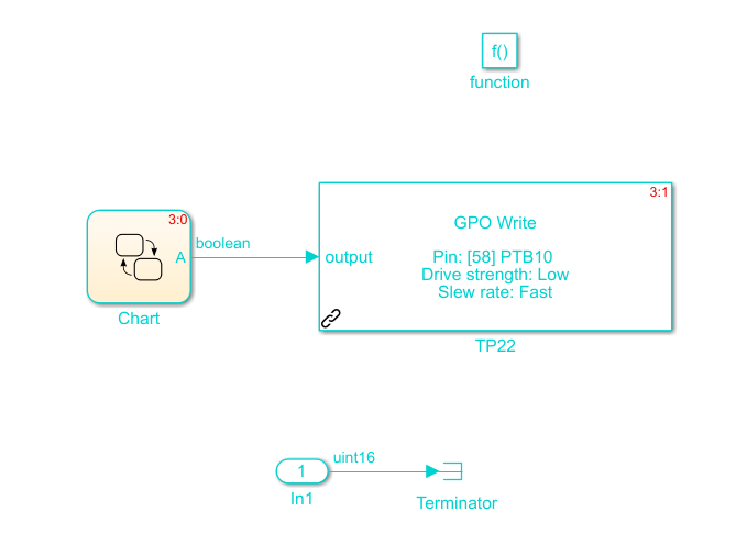
This is the Image I'm talking about. Your testpin (yellow) switches on for a short Moment (a pulse of something like 4us) with falling edge PWM command Cyan.
My testpin only Switches the state with every falling edge of pwm, so it requires something to Switch back without having a new Trigger Input.
Does this make it more understandable what I mean ?
Best regards
Leon
- Mark as New
- Bookmark
- Subscribe
- Mute
- Subscribe to RSS Feed
- Permalink
- Report Inappropriate Content
I have found out that the eFlexPWM Interrupt works if I use three complementary pwm Output blocks (module 0, module 1 and module 2) instead of one three Phase Output block... is that a bug ?
