- NXP Forums
- Product Forums
- General Purpose MicrocontrollersGeneral Purpose Microcontrollers
- i.MX Forumsi.MX Forums
- QorIQ Processing PlatformsQorIQ Processing Platforms
- Identification and SecurityIdentification and Security
- Power ManagementPower Management
- MCX Microcontrollers
- S32G
- S32K
- S32V
- MPC5xxx
- Other NXP Products
- Wireless Connectivity
- S12 / MagniV Microcontrollers
- Powertrain and Electrification Analog Drivers
- Sensors
- Vybrid Processors
- Digital Signal Controllers
- 8-bit Microcontrollers
- ColdFire/68K Microcontrollers and Processors
- PowerQUICC Processors
- OSBDM and TBDML
-
- Solution Forums
- Software Forums
- MCUXpresso Software and ToolsMCUXpresso Software and Tools
- CodeWarriorCodeWarrior
- MQX Software SolutionsMQX Software Solutions
- Model-Based Design Toolbox (MBDT)Model-Based Design Toolbox (MBDT)
- FreeMASTER
- eIQ Machine Learning Software
- Embedded Software and Tools Clinic
- S32 SDK
- S32 Design Studio
- Vigiles
- GUI Guider
- Zephyr Project
- Voice Technology
- Application Software Packs
- Secure Provisioning SDK (SPSDK)
- Processor Expert Software
-
- Topics
- Mobile Robotics - Drones and RoversMobile Robotics - Drones and Rovers
- NXP Training ContentNXP Training Content
- University ProgramsUniversity Programs
- Rapid IoT
- NXP Designs
- SafeAssure-Community
- OSS Security & Maintenance
- Using Our Community
-
-
- Home
- :
- Model-Based Design Toolbox (MBDT)
- :
- Model-Based Design Toolbox (MBDT)
- :
- Re: How to read SPI message from the PowerSBC chip MC33FS6522LAE on the Devkit MPC5744P-Rev.E using MBD toolbox
How to read SPI message from the PowerSBC chip MC33FS6522LAE on the Devkit MPC5744P-Rev.E using MBD toolbox
- Subscribe to RSS Feed
- Mark Topic as New
- Mark Topic as Read
- Float this Topic for Current User
- Bookmark
- Subscribe
- Mute
- Printer Friendly Page
- Mark as New
- Bookmark
- Subscribe
- Mute
- Subscribe to RSS Feed
- Permalink
- Report Inappropriate Content
Hello,
I am using the Devkit MPC5744P Rev E and the Model Based Design Toolbox 3.0.0.
I would like to read a simple message from the PowerSBC chip MC33FS6522LAE, which is connected to the micro-controller by SPI0. This SPI message is 16 bits size.
Can anyone help me with it?
Attached follows the model, which I am trying to send a read request, but I am getting no feedback.
Also a picture of the board jumpers configuration.
Regards, Rafael
abhishek.kumar@chassisbrakes.com
Solved! Go to Solution.
- Mark as New
- Bookmark
- Subscribe
- Mute
- Subscribe to RSS Feed
- Permalink
- Report Inappropriate Content
Hello rafael.barbosa@chassisbrakes.com,
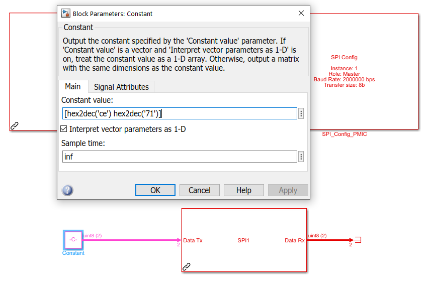
When using the 2 constant blocks and 1 mux (like in your example), I was able to reproduce your error. What happened in this case is Simulink coder saw that variable as if it was only 1B instead of 2B. I was able to get the desired output on SPI using a constant block, as shown in the image below (using an array of 2 uint8_t variables, 0xCE and 0x71).
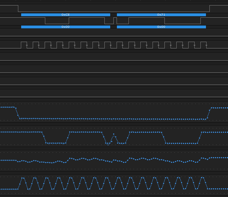
This is the output I am getting:
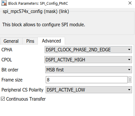
I am transmitting 0xCE71 in 1 transfer, using the following options:
Note that the MOSI is still going up (at about 1.8V) for ~0.12us, but due to the sampling of data being done on the trailing edge of the clock, this does not impact the message. This issue will be sorted out with the SDK team - when they will have reached to a conclusion I will let you know.
Also note that this has been done with the PEBRIDGE set to 50MHz (but no notable difference versus the old configuration).
Kind regards,
Razvan.
- Mark as New
- Bookmark
- Subscribe
- Mute
- Subscribe to RSS Feed
- Permalink
- Report Inappropriate Content
Hello constantinrazvan.chivu, adriantudor and mariuslucianandrei
Using the Frame Size configuration = 8 with Continuous Transfer to send some "Read Command", I still get some response via SPI (As already stated previously for the SPI Device ID message).
However, when I try to send some "Write command", I directly get an error.
As example I am trying to send the WD_WINDOW command to configure the watchdog window duration to 12 ms (SPI output message 0xCE71).
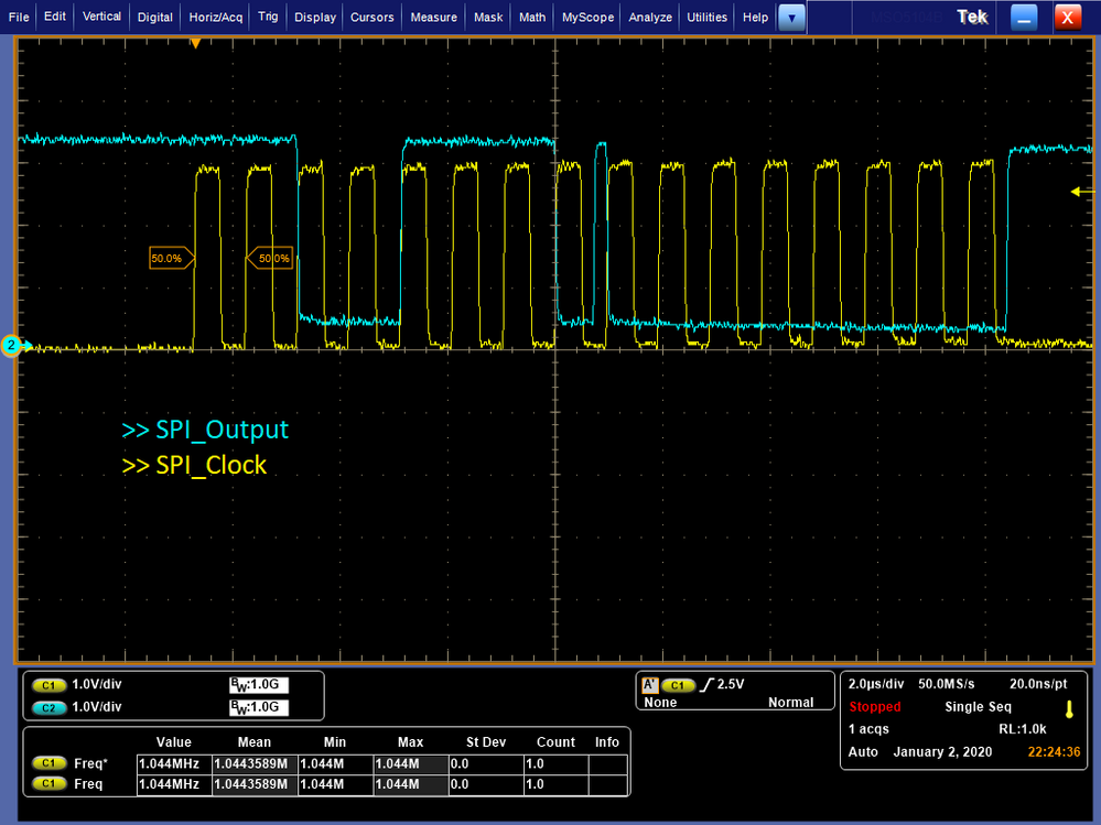
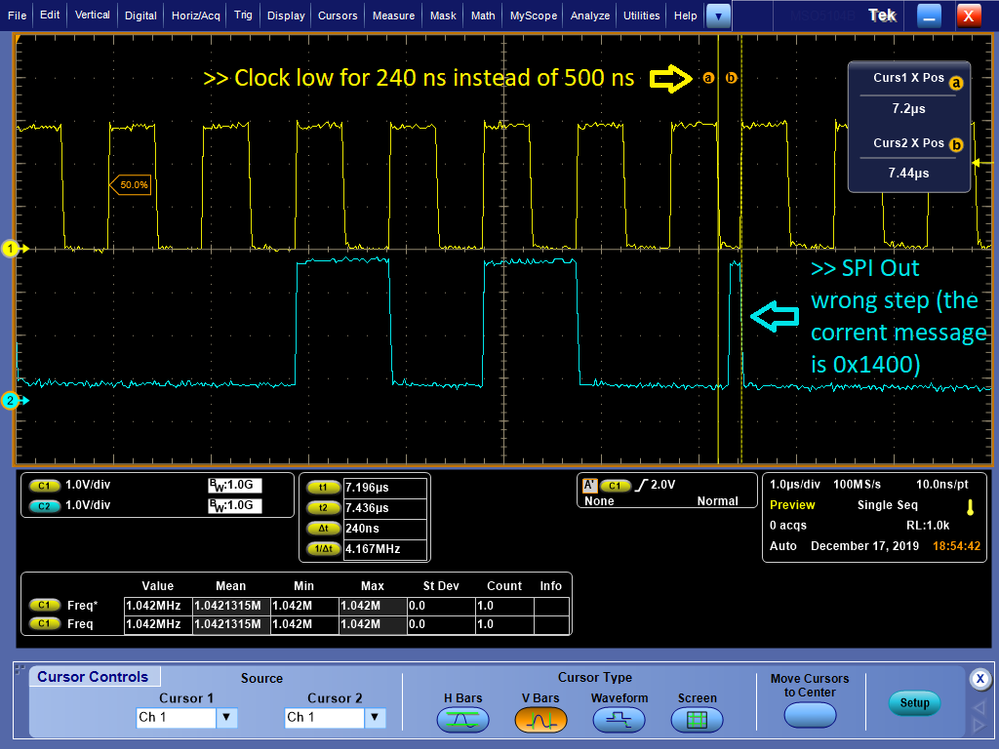
Watching the SPI_Output on oscilloscope, it seems to be sending the message 0xCE00 (What causes a SPI error):
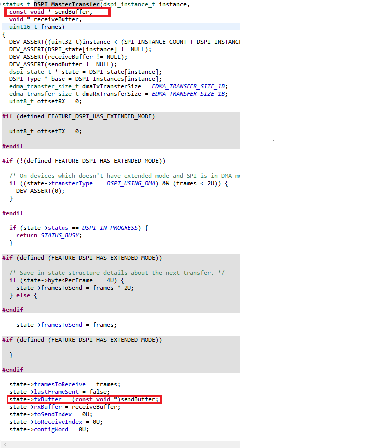
By checking the generated code, the DSPI_MASTER_TRANSFER function sends the SPI output when called.
Function Call:
Local Variable:
Values in memory:
I believe some problem is going on.
I imagine that the bytes of the command 0xCE71 shall be placed consecutive in the memory in order to send the data to the SPI transmit buffer.
What do you think?
Please let me know a solution as soon as possible.
Regards, Rafael
- Mark as New
- Bookmark
- Subscribe
- Mute
- Subscribe to RSS Feed
- Permalink
- Report Inappropriate Content
Hello rafael.barbosa@chassisbrakes.com,
When using the 2 constant blocks and 1 mux (like in your example), I was able to reproduce your error. What happened in this case is Simulink coder saw that variable as if it was only 1B instead of 2B. I was able to get the desired output on SPI using a constant block, as shown in the image below (using an array of 2 uint8_t variables, 0xCE and 0x71).
This is the output I am getting:
I am transmitting 0xCE71 in 1 transfer, using the following options:
Note that the MOSI is still going up (at about 1.8V) for ~0.12us, but due to the sampling of data being done on the trailing edge of the clock, this does not impact the message. This issue will be sorted out with the SDK team - when they will have reached to a conclusion I will let you know.
Also note that this has been done with the PEBRIDGE set to 50MHz (but no notable difference versus the old configuration).
Kind regards,
Razvan.
- Mark as New
- Bookmark
- Subscribe
- Mute
- Subscribe to RSS Feed
- Permalink
- Report Inappropriate Content
Dear constantinrazvan.chivu
Thank you, the example worked fine with the constants like you mentioned.
Kind Regards, Rafael
- Mark as New
- Bookmark
- Subscribe
- Mute
- Subscribe to RSS Feed
- Permalink
- Report Inappropriate Content
Hello constantinrazvan.chivu,
Indeed the configuration is 16 bits and the transmit is a mux with two sets of 8 bits.
But I had to use this approach because the SPI Transfer block just accept uint8 input datatype.
Also I tried to run the example with the configuration frame size 8 and continuous transfer
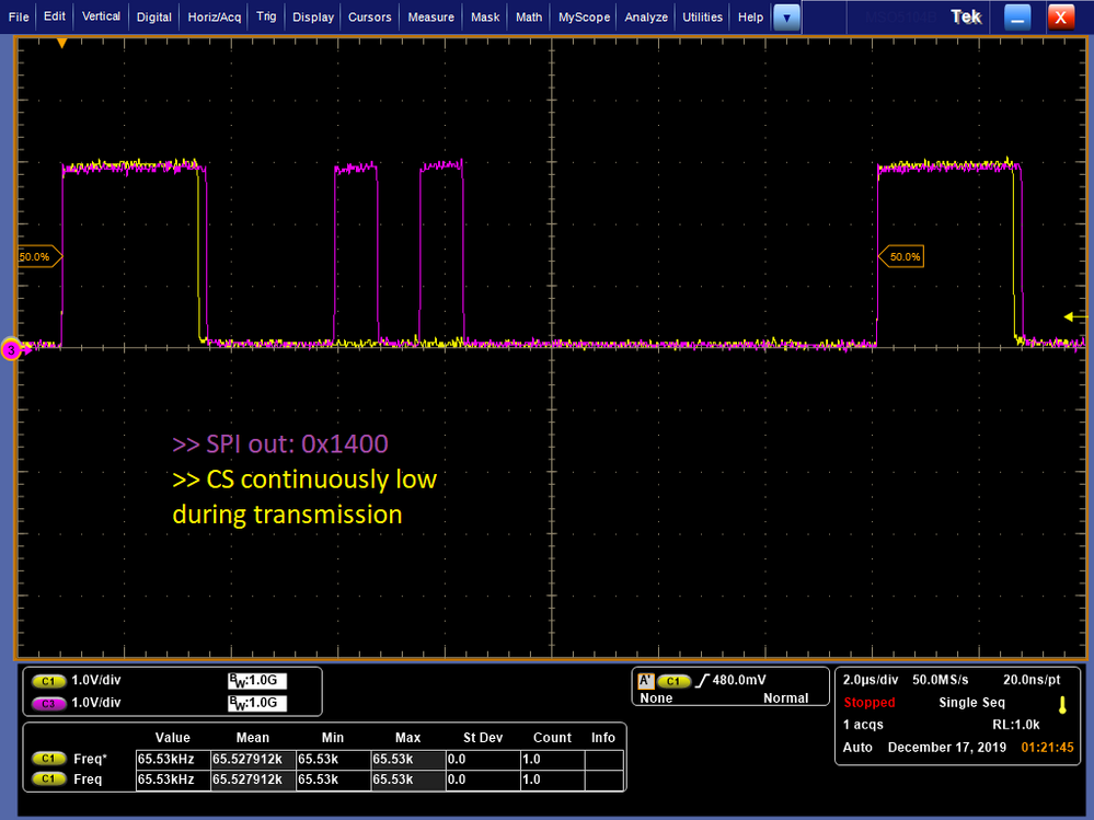
but still there is a unexpected behavior in the SPI output, as you can see below: The SPI message is 0x1400. There is a unexpected step (the last one).
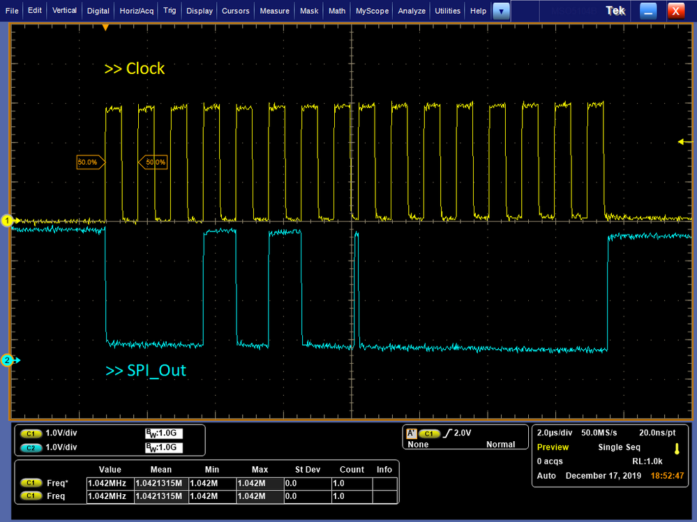
Also you can check the strange clock behavior during the transmission on the below picture:
Kind Regards, Rafael
- Mark as New
- Bookmark
- Subscribe
- Mute
- Subscribe to RSS Feed
- Permalink
- Report Inappropriate Content
I just attached the 8 bits and continuous SPI configuration on the first question.
- Mark as New
- Bookmark
- Subscribe
- Mute
- Subscribe to RSS Feed
- Permalink
- Report Inappropriate Content
Hello rafael.barbosa@chassisbrakes.com,
I saw the rest of your messages after I posted my last reply - I saw that in my own example as well - that is indeed strange.
In my case it goes to around 2V4, so it does not reach ~3v2 as the valid data does. adriantudor suggested that it might be due to MOSI pin being undriven for a small period of time, while having a pullup. This can cause the pin to start going up, then the SPI starts driving it again. I will investigate this behavior, but in your case, having the clock phase set to the trailing edge (2nd edge) and the clock polarity to active high, that part of data will not be sampled (so it is read as '0' even though the logic analyzer clearly catches it).
Kind regards,
Razvan.
- Mark as New
- Bookmark
- Subscribe
- Mute
- Subscribe to RSS Feed
- Permalink
- Report Inappropriate Content
Hello constantinrazvan.chivu,
I could check a wrong configuration on the PBRIDGE clock, which is the base for the SPI clock.
The MBD Toolbox generates code with PBRIGDE frequency of 100MHz, but the maximum shall be 50MHz.
To see better explanation, please check the following topic:
https://community.nxp.com/message/1250768
Running the examples using a proper configuration for PBRIGDE clock (max of 50 MHz) may improve something but still doesn't solve the problem.
Regards, Rafael
- Mark as New
- Bookmark
- Subscribe
- Mute
- Subscribe to RSS Feed
- Permalink
- Report Inappropriate Content
Hello rafael.barbosa@chassisbrakes.com,
As I answered in the PEBRIDGE question, I will investigate and provide a fix (for the correct clock value). Afterwards I will investigate this issue as well.
We just came back to office, so it might take longer than expected as we have questions/issues piled up; thank you for understanding!
Kind regards,
Razvan.
- Mark as New
- Bookmark
- Subscribe
- Mute
- Subscribe to RSS Feed
- Permalink
- Report Inappropriate Content
Hello constantinrazvan.chivu,
Thank you for the message.
Do you already have some updating regarding this issue?
Kind regards, Rafael
- Mark as New
- Bookmark
- Subscribe
- Mute
- Subscribe to RSS Feed
- Permalink
- Report Inappropriate Content
Just to explain a bit better the impact of this transmit strange behavior:
Taking as example the read command: SPI Device ID (0x1400),to the MC33FS6522LAE device
The expected input response is: 0x08F2 (Response get by the C code example from S32 Design Studio).
It means: No error, just the IO_G active.
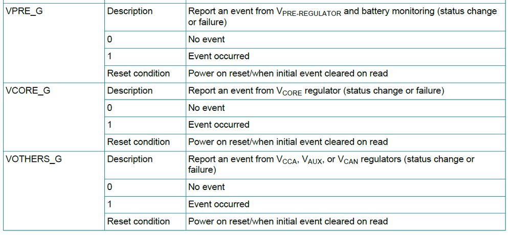
Using the Frame Size configuration = 16, I got the response: 0x8FF2,
Which means SPI_G error and the fields VPRE_G, VCORE_G and VOTHERS_G active.
After using the Frame Size configuration = 8 with continuous transfer, I got the response: 0x0FF2.
The SPI_G error is not triggering anymore.
However the fields VPRE_G, VCORE_G and VOTHERS_G are still active.
That is it.
Kind Regards, Rafael
- Mark as New
- Bookmark
- Subscribe
- Mute
- Subscribe to RSS Feed
- Permalink
- Report Inappropriate Content
Dears constantinrazvan.chivu and adriantudor,
Thank you for the support.
Please let me know when you have some updating after your investigation.
Kind Regards, Rafael
- Mark as New
- Bookmark
- Subscribe
- Mute
- Subscribe to RSS Feed
- Permalink
- Report Inappropriate Content
Hello rafael.barbosa@chassisbrakes.com,
We will let you know, but it might take a while as we'll be out of office for 2 weeks starting from 23 December (Christmas Holiday) - so if we don't answer by tomorrow, there will be a longer wait time.
Kind regards,
Razvan.
- Mark as New
- Bookmark
- Subscribe
- Mute
- Subscribe to RSS Feed
- Permalink
- Report Inappropriate Content
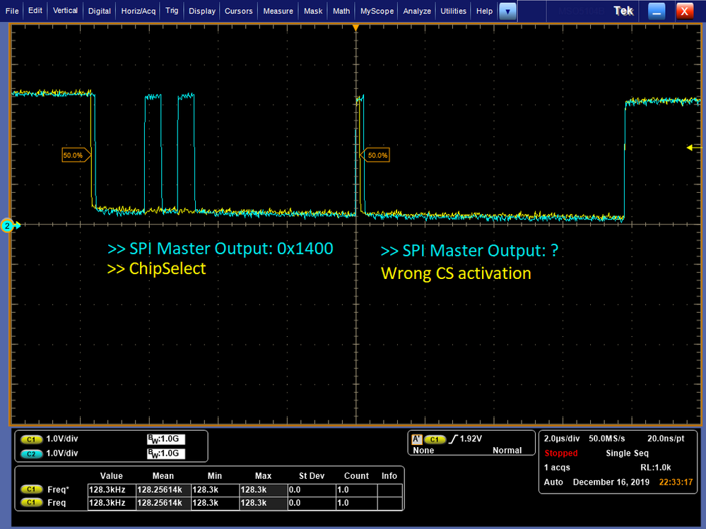
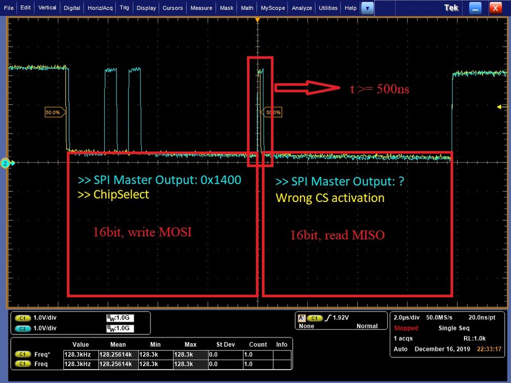
Hello, I would like to share some screenshots that show out what is the behavior of Chip select, Clock and SPI Output for the model sent attached on previous message
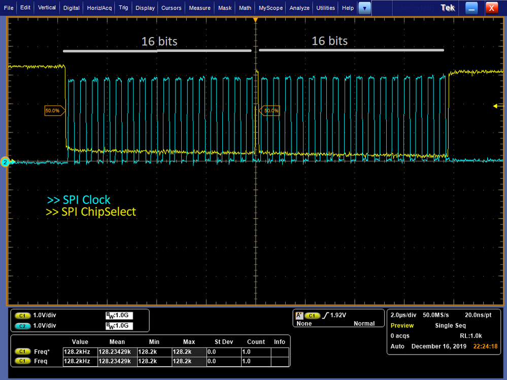
From my understanding the output of CS has a wrong activation after sending the message.
Probably it is causing error when reading the message.
Can anyone support me with it?
Kind Regards, Rafael
- Mark as New
- Bookmark
- Subscribe
- Mute
- Subscribe to RSS Feed
- Permalink
- Report Inappropriate Content
Hi Rafael Barbosa,
In order to read registers/messages from SBC you must requested data thru MOSI, wait more than 500 ns, then read MISO.
Best regards,
Adrian
- Mark as New
- Bookmark
- Subscribe
- Mute
- Subscribe to RSS Feed
- Permalink
- Report Inappropriate Content
Hello adriantudor,
Thank you for the response.
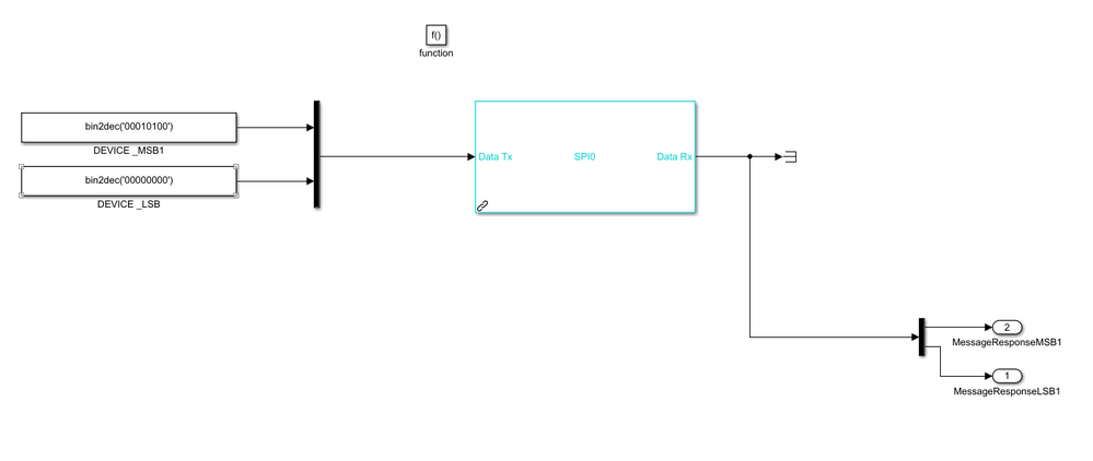
I don't know if you had a chance to look into the .zip file that I sent on the first post, but I am using the MBD implementation to send the reading command:
From this implementation with the used SPI configuration, I expected to see just the firsts 16 bits. The seconds set of 16 bits are not expected.
Regards, Rafael
- Mark as New
- Bookmark
- Subscribe
- Mute
- Subscribe to RSS Feed
- Permalink
- Report Inappropriate Content
Hello rafael.barbosa@chassisbrakes.com,
The SPI Transfer block sets the transfer size equal to the width of the input signal. Simulink mux block outputs uint8[2] signal, so it is actually setting the transfer size to 2, thus the signal you get (2 x transfer size, with CS being reactivated between the 2).
I will give you a model that will generate the signal that you are looking for.
Kind regards,
Razvan.
P.S.: Thank you adriantudor for the help on this matter!
- Mark as New
- Bookmark
- Subscribe
- Mute
- Subscribe to RSS Feed
- Permalink
- Report Inappropriate Content
Hello rafael.barbosa@chassisbrakes.com,
So the easiest way (minimum of change to your model) would be to change the SPI settings from the SPI Config block. Set
frame size = 8
and enable
Continuous transfer
to get the following signal:
Let me explain why these settings: on one hand, you'll have transfer size set to 2 (due to usage of MUX block); on the other hand, you want to send 16bits. Given this context, you can only set the frame size to 8. After you have these settings, you only need to enable continuous transfer so that you don't have the CS go HIGH in the middle of the 2 bytes.
There are other ways for achieving the same end result, but being necessary to change more blocks in your model, I don't see it become relevant.
The easiest way in managing any kind of SPI transfer is by using 8bit frame size with cointinuous transfer enabled and making sure you give the SPI T'ransfer block an input of appropriate size (the transfer size you need).
Please let me know if you have other questions regarding this subject.
Kind regards,
Razvan.
- Mark as New
- Bookmark
- Subscribe
- Mute
- Subscribe to RSS Feed
- Permalink
- Report Inappropriate Content
Hello rafael.barbosa@chassisbrakes.com,
I will take a look at your model but first lets clarify what you are trying to achieve - do you want to CS to remain low for the duration of the whole 16+16 bits transfer? Or what is the desired signal output?
Kind regards,
Razvan.
- Mark as New
- Bookmark
- Subscribe
- Mute
- Subscribe to RSS Feed
- Permalink
- Report Inappropriate Content
Hello Razvan,
Thank for the response.
The target is to read a simple SPI message of 16 bits size using the MBD.
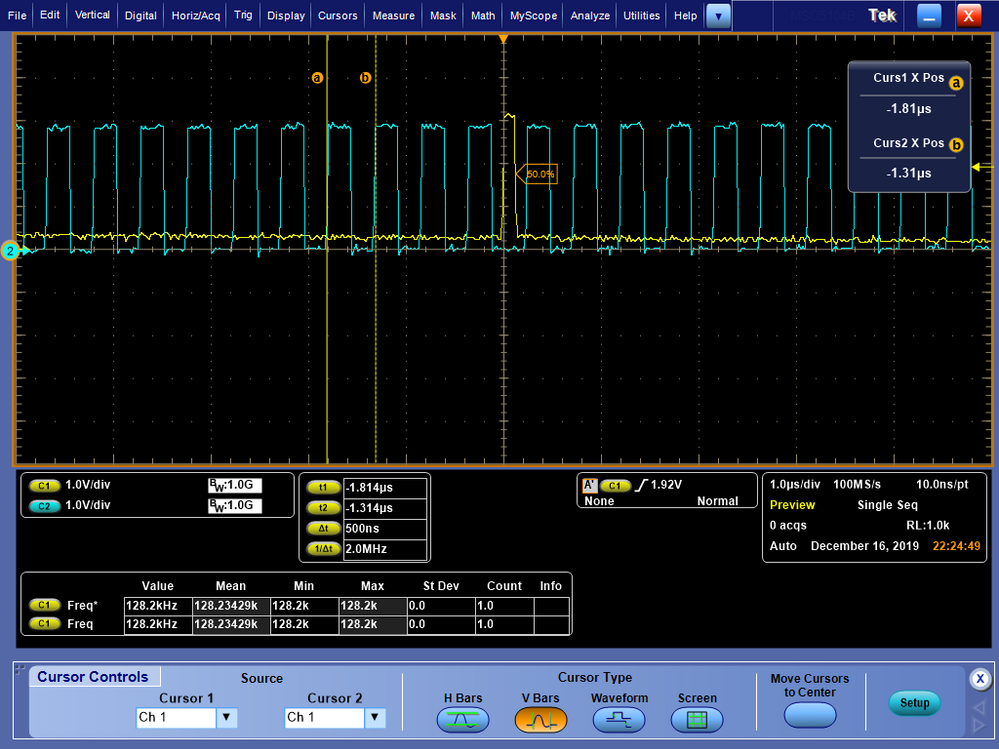
Below you can see a correct message output using the example from S32 Design Studio (direct C code).
Kind Regards, Rafael Barbosa
