- NXP Forums
- Product Forums
- General Purpose MicrocontrollersGeneral Purpose Microcontrollers
- i.MX Forumsi.MX Forums
- QorIQ Processing PlatformsQorIQ Processing Platforms
- Identification and SecurityIdentification and Security
- Power ManagementPower Management
- MCX Microcontrollers
- S32G
- S32K
- S32V
- MPC5xxx
- Other NXP Products
- Wireless Connectivity
- S12 / MagniV Microcontrollers
- Powertrain and Electrification Analog Drivers
- Sensors
- Vybrid Processors
- Digital Signal Controllers
- 8-bit Microcontrollers
- ColdFire/68K Microcontrollers and Processors
- PowerQUICC Processors
- OSBDM and TBDML
-
- Solution Forums
- Software Forums
- MCUXpresso Software and ToolsMCUXpresso Software and Tools
- CodeWarriorCodeWarrior
- MQX Software SolutionsMQX Software Solutions
- Model-Based Design Toolbox (MBDT)Model-Based Design Toolbox (MBDT)
- FreeMASTER
- eIQ Machine Learning Software
- Embedded Software and Tools Clinic
- S32 SDK
- S32 Design Studio
- Vigiles
- GUI Guider
- Zephyr Project
- Voice Technology
- Application Software Packs
- Secure Provisioning SDK (SPSDK)
- Processor Expert Software
-
- Topics
- Mobile Robotics - Drones and RoversMobile Robotics - Drones and Rovers
- NXP Training ContentNXP Training Content
- University ProgramsUniversity Programs
- Rapid IoT
- NXP Designs
- SafeAssure-Community
- OSS Security & Maintenance
- Using Our Community
-
-
- Home
- :
- Model-Based Design Toolbox (MBDT)
- :
- NXP Model-Based Design Tools Knowledge Base
- :
- Create an Autonomous Intelligent Self Driving Car for NXP Cup with S32K Model-Based Design Toolbox
Create an Autonomous Intelligent Self Driving Car for NXP Cup with S32K Model-Based Design Toolbox
- Subscribe to RSS Feed
- Mark as New
- Mark as Read
- Bookmark
- Subscribe
- Printer Friendly Page
- Report Inappropriate Content
Create an Autonomous Intelligent Self Driving Car for NXP Cup with S32K Model-Based Design Toolbox
Create an Autonomous Intelligent Self Driving Car for NXP Cup with S32K Model-Based Design Toolbox
 |
1. Introduction
1.1 A New Control Option For NXP Cup Race Car
NXP Cup car development kit is usually based on NXP's Freedom KL25Z board for motors control and image evaluation. However the control of the race car can be done with multiple NXP solutions.
In this article, a solution based on S32K144EVB board will be presented along with a programming approach based on MATLAB/Simulink Model-Based Design Toolbox for S32K. Additionally another tool provided by NXP - FreeMASTER - will be used to debug in real time the application.
As S32K144 pinout is not compatible with the default Landzo board pinout, an additional board to route the pins to the desired destination has been built. Complete details on the mapping of the pins are provided in the tutorial.
This article is structured as a tutorial detailing all the steps and providing all the source code to enable one to use this solution. However the control application is done very simple - on purpose - and uses just 10% of the speed to prove the concept.
Table 1. Freedom KL25Z vs. S32K144 features | ||||||||||||||||||||
|
1.2 Resources
- Model-Based Design Toolbox – Tool used to create complex applications and program the S32K144 MCU directly from the MATLAB/Simulink environment. This tool allows automatic code generation for S32K144 peripherals based on configuration of the Simulink model done by the user.
- S32K144-Q100 Evaluation Board – Evaluation board from the S32K14x family used for quick application prototyping and demonstration.
- NXP Cup Development Kit – Information about the hardware components of the development kit and instructions regarding the car assembling. Software which is helpful for the project design is also presented.
- FreeMaster Debugging Tool – Real-time data monitor tool which shows in both graphical mode (as a scope for example) and text mode the evolution of variables in time. It is suitable to monitor application behavior in real time during execution of the code.
- TSL1401 Datasheet – Information regarding the camera configuration.
- Excel Spreadsheet (attached at the end of the document) with routing information to map pins from Landzo to S32K144 board.
2. Hardware Setup
After assembling all the hardware modules as indicated in the development kit the car will look like in the next image. It should be mentioned that for the S32K144 EVB to system board connection an S32K adapter board was created.
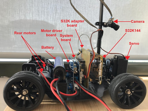 |
Fig 1. Hardware setup |
2.1 Hardware Modules
The hardware modules of this application and the way the peripherals of the S32K144 MCU are communicating with those is summarized in the Fig. 2. To understand more about the control of the motors, please check chapters 3.4.4 and 3.4.5. For learning how to debug the application using the Freemaster software, take a look at the chapter 4 where a detailed description is presented. A similar indication is given also for the camera information collecting. Chapter 3.4.1 and 3.4.2 provide a close-up image of the operations that need to be done in order to make the car “see”.
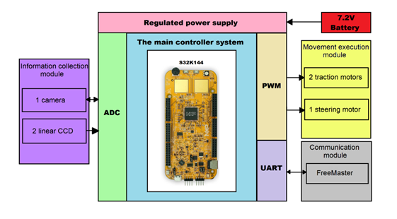 |
| Fig 2. System block diagram |
2.2 Hardware Validation Steps
After connecting all the hardware modules, connect a USB cable to the PC. Connect other end of USB cable to mini-B port on FRDM-KEA at J7. When powered through USB, LEDs D2 and D3 should light green like in the picture below. Also, once the S32K144 board is recognized, it should appear as a mass storage device in your PC with the name EVB-S32K144.
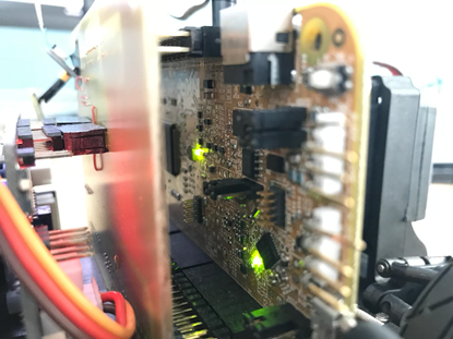 |
Fig 3. LEDs to validate the correct setup |
3. Model-Based Design Application
3.1 Application Description
The Model-Based Design approach consists of a visual way of programming, which is based on blocks. A block implements a certain functionality, such as adding two numbers. In case of the NXP's Model-Based Design Toolbox which is specifically developed for the S32K14x family, a block implements a functionality of a MCU peripheral, such as turning on the green led on the board. Each block has a different functionality and for a complex application, multiple components should be used together so they can provide the best solution for the problem proposed. For example, if you want to toggle the green led at every 10 seconds, you are going to add a new block to your design, one that can count those 10 seconds and then trigger an action when the count is over, which is toggling the led. Connection between the blocks should be made accordingly to your application system model. When building the model, the code that stands behind the blocks and implements the connection logic between them is automatically generated and downloaded on the embedded target. Doing so, code errors are certainly eliminated, and a faster design process is accomplished.
For using the Model-Based Design Toolbox for S32K, the MATLAB programming platform should be installed on the PC you are working on. Make sure that you respect all the System Requirements that you can find on the following link (Model Based Design Toolbox). Follow the installation steps from the Install and Configuration Steps and now you are ready to develop your own model-based design application.
3.2 Application Scheme
The generated code from the Simulink model is downloaded on the S32K144 MCU. A mapping between hardware and software for this application is illustrated in the figure below:
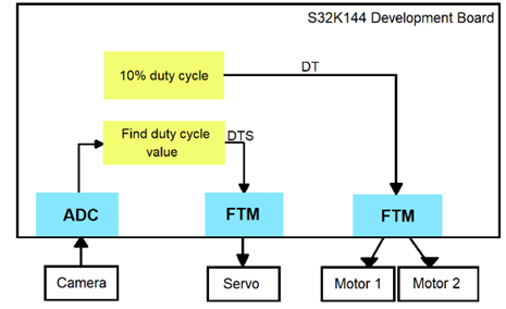 |
Fig 4. Hardware to software mapping |
The hardware components are controlled by the application through the peripheral functions of the S32K144 MCU. This board is connected to the other hardware modules by using an adapter board. In the link NXP Cup Development Kit there are information regarding how to connect the camera, servo and motors modules on the System and Driver Boards. Thus, the software generated signals are transmitted to the modules that need to be configured and controlled (camera, servo, motors).
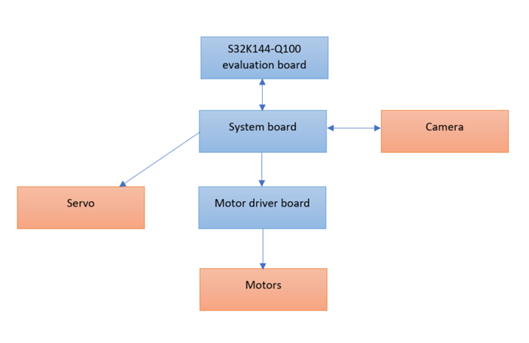 |
Fig 5. Application Scheme |
When you open the Simulink model, this structure shown in Fig. 6 will be displayed. The functionalities are grouped in areas, which area containing a small description of what it is computed inside it. There are blocks and connections between them like mentioned before. Based on the image given by the camera, the steering and the speed of the car should be controlled. More details about how each of the subsystems works are provided in the following chapters.
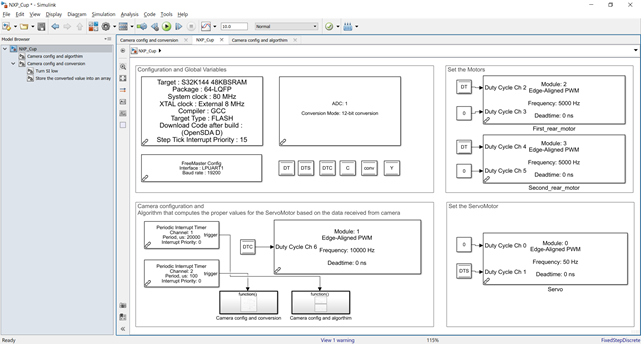 |
Fig 6. Simulink top level system |
3.3 Application Logic
The application logic is described by the following block diagram. The signal from the camera is converted and the data is stored in an array. Based on the elements of the array (description of the image in front of the car), an algorithm will compute how much does the car have to steer its front wheels. This is expressed in a duty cycle value of a signal, signal which will be directly transmitted to the servo module. A constant speed, 10% of the maximum reachable of the car, it is also given as a duty cycle of the signal which will control the two rear motors.
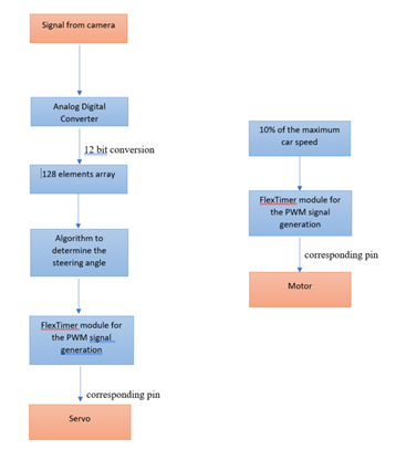 |
Fig 7. Application logic diagram |
3.4 Simulink Model Components
3.4.1 Camera Configuration
The camera module has a major importance in the project, because it is used to scan and process the track in front of the car. Firstly, for the main purpose of the application: control the car and maintain its position on the desired direction, the camera module should be configured so it can receive the analog signal properly. After the camera receives the analog signal, the application converts it into 128 digital values on the basis of which control decisions will be taken. There are 128 digital values for a conversion because the line scan camera module consists of a linear sensor array of 128 pixels and an adjustable lens. As specified in the datasheet, for the camera module configuration, two signals must be generated, a clock and a serial input (CLK and SI).
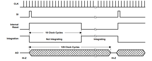 |
| Fig 8. Waveforms for camera configuration |
To validate the functionality of this module, you should open the FreeMaster and check that the camera is working properly. Open the .pmp file and watch the conv variable evolving on the recorder. Put a white paper in front of your camera and then move an object in front of it. Every time the camera spots a dark color, its graphical evolution presents easy observable dips like in the picture below (blue graphic).
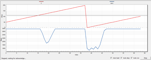 |
Fig 9. Dips caused by dark objects |
CLK Signal
For the CLK signal generation, a FTM (FlexTimer) block is used. This block generates a PWM signal with a duty cycle given as an input (DTC – Dutcy Cycle Camera). The duty cycle has to be 0.5 (50%) as specified in the datasheet. The PWM signal is then passed to the corresponding pin of the camera module through the S32K144 board. Check the Landzo_car pins to S32K144EVB file for the mapping and connections.
The frequency of the clock signal was chosen considering the imposed value range in the datasheet. (fclock between 5 and 2000 kHz).
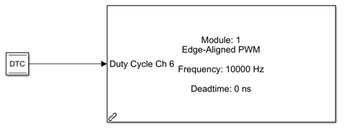 |
Fig 10. Generating the CLK signal |
When configuring the FTM block, the following block parameters will be available:
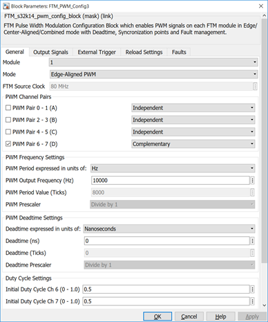 |
Fig 11. FTM block parameters |
The FTM functionality has 4 different modules, each of them with 8 channels grouped in pairs (for each channel an output pin can be selected). After checking the Landzo_car pins to S32K144EVB file for the corresponding pin of the camera CLK, the choice of the FTM module and the pair should be done (FTM0_CH1 means that the pin is connected to the FTM0 module, pair 0-1). It should also be mentioned that the camera module is connected on the CCD1 interface of the System Board in the hardware setup of this application. Another linear interface CCD2 is available for user usage, as specified in the description of the development kit. The frequency of the signal can also be set from the editbox in the Frequency Settings groupbox. An initial duty cycle value equal to 0.5 was set according to the datasheet.
There are two operation modes for each pair of channels and they can be chosen from the popup box next to the pair selection. These modes are called independent and complementary. Let’s give them a short description.
By setting channel n in the Complementary mode, the output for the channel n+1 will be the inverse of the channel n output and the block will have only one input. In the Independent mode, the channels have independent outputs, each one depending on the duty cycle given as an input on that channel (2 inputs for the block in this case). The CLK signal of the camera is transmitted to a single pin of the hardware module, so there is no need for two channels to be configured. Only one is enough to output the desired waveform (in complementary mode, only the first channel of a pair will be set; ex: channel 0, channel 2, channel 4, channel 6). That is why the Complementary option is chosen in this case. The input will be the 50% duty cycle on the basis of which the CLK signal will be generated. The channel 7 will now be the inverse of the channel 6 but in the next picture it can be observed that the channel 7 does not have a pin to output the signal to, because the inverted CLK signal is not needed in the current application.
 |
Fig 12. FTM output signals |
SI Signal
The SI signal’s period must provide enough time for 129 CLK cycles, as the timing requires (datasheet). 129 CLK cycles are needed with the purpose of acquiring 128 samples of the analog signal received by the camera. In order to meet all the specified conditions for a normal operation mode, the algorithm to create the CLK and SI waveforms as required uses two Periodic Interrupt Timers (PIT) blocks.
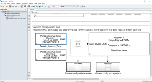 |
| Fig 13. PIT blocks |
An interrupt represents a signal transmitted to the processor by hardware or software indicating an important event that needs immediate attention. The processor responds to this signal by suspending its current activities, saving its state and executing a function called an interrupt handler to deal with the event. The interruption is temporary, and, after the interrupt handler finishes, the processor resumes its normal activities.
A PIT block is used to trigger an interrupt handler to execute at every timeout of a counter. The Function-Call Subsystems linked to the PIT blocks represent the actions inside the interrupt handler. The interrupt handler will be triggered every Period(us). For the first PIT, it will be triggered every 20000us and for the second one every 100us. This means that every time the counter reaches the value specified in the block configuration parameters, the Function-Call Subsystem is triggered, the actions inside of it executed and the counter reinitialized.
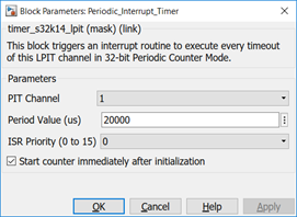 |
| Fig 14. PIT block parameters |
The PIT functionality has 4 channels, and they are implemented based on independent counters. The channel 0 is not available for user usage because it is configured to trigger the execution of the entire model at every period of time specified in the model configuration parameters.
The last checkbox from the block parameters is used to start the counter immediately after the application initialization, without waiting for other events.
Considering all the information mentioned above, the timing of creating the waveforms as required involves the following actions:
- at every 100µs (CLK signal’s period) the next things happen:
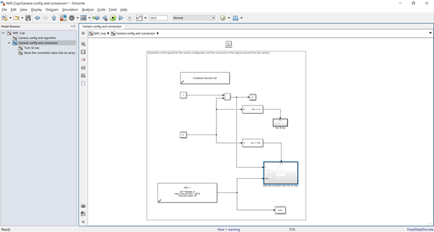 |
Fig 15. Actions in the 100us interrupt |
- C variable, which counts the clock cycles, is incremented;
- If C >=2, the SI signal is turned from high to low. (value 2 was chosen to keep the SI signal high for the convenient amount of time as specified by the tw, tsu, th and ts parameters. Their values can be found in the datasheet)
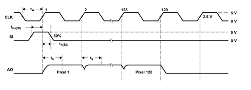 |
Fig 16. Timing for camera configuration |
A GPIO (General Purpose Input/Output) block is used for this and its role is to send the value given as an input to the selected pin which can be selected from the dropdown menu available in the block configuration parameters).
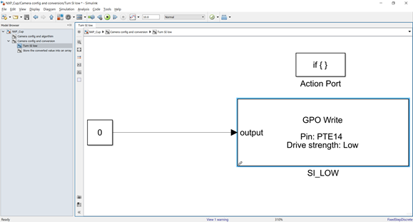 |
| Fig 17. Setting SI signal LOW |
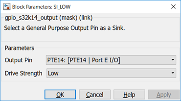 |
Fig 18. GPIO block parameters |
- A conversion is started and if C < 128, the converted values (analog-digital conversion of the received signal from the camera) are stored in an array of 128 elements (Store the converted values into an array subsystem is triggered) and into the conv array. Conv variable is used for the debugging process which will be later detailed.
- at every 20ms (SI signal’s period) the next things happen:
- SI signal is turned from low to high using the same GPIO functionality;
- The clock cycles counter C is reinitialized;
- Based on the values of the array (high values for white, low values for dark) and on their indexes, the duty cycle (DTS – Duty Cycle Servo) which controls the Servo is computed (it controls the car to turn left or right with a certain angle);
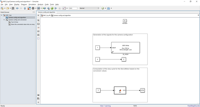 |
Fig 19. Actions in the 20ms interrupt |
3.4.2 Camera Reading
After the camera module is configured (SI and CLK signals generated as specified), the data acquisition can be started. The signal given by the camera is converted into digital values which are stored in an array. The conversion implies the usage of the ADC (Analog to Digital Converter) functionality. Taking this into consideration, a configuration block for the ADC should be added to the Simulink model.
 |
Fig 20. ADC configuration block |
The ADC of the S32K144 has two modules (ADC0, ADC1) each of them with up to 16 external analog input channels and up to 12-bit conversion resolution. The camera module is connected to the CCD 1 linear interface of the System Board. The Landzo_car pins to S32K144EVB file specifies that the pin of the camera module which receives the analog signal is ADC1_CH10, so the ADC 1 module should be configured. A 12-bit conversion resolution was chosen for improving the accuracy of the sampled data.
An analog to digital conversion should happen every 100us as specified in the Timing section, because 128 samples of the input signal need to be acquired (every time the C variable is incremented, a value should be stored in the conversion array).
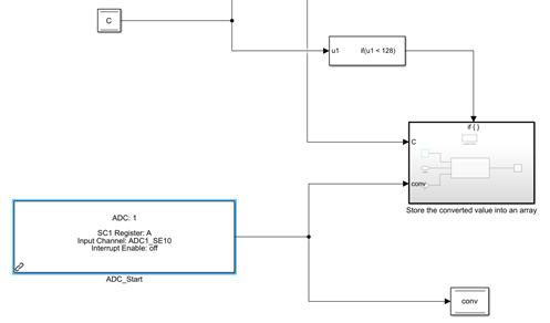 |
Fig 21. Start of conversion |
Considering the facts mentioned in the previous paragraph, every time the subsystem of the PIT block is triggered, the conversion is started (an ADC Start block is used) and if C < 128 the sampled data is stored into the array that will consist the information on which basis the servo control decision will be taken. Variable C is the index of the array elements and each result of the conversion represents the value of an element. Following this algorithm, the Y array is created and it is going to be used in the next chapter where the algorithm which computes how much the car should steer, based on the image of the track in front of it, is described. For putting the values into the array an assignment block is used.
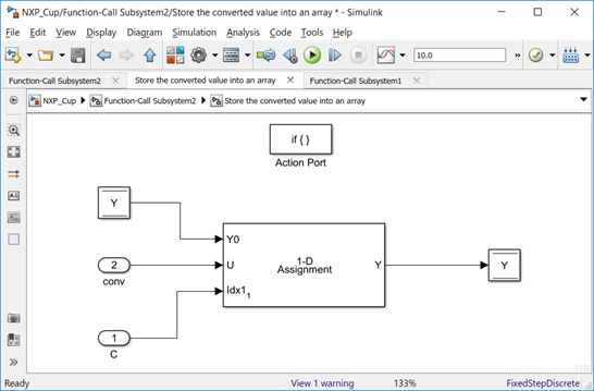 |
| Fig 22. Storing conversion values to Y array |
3.4.3 Camera To Steering Algorithm
The algorithm presents a basic approach and uses an if-else logic. Before giving it a short description, a couple of things should be mentioned.
- Considering the reference voltage of the ADC module of the microcontroller which is 5V and the 12 bit resolution of the conversion, the resolution on a quantum is 5 / 4095. But the camera is powered by a voltage approximately equal to 3.4V, thus resulting a value which varies around 3.4 / ( 5/4095) = 2785. This value is the maximum that the ADC can provide when the camera spots white in front of it. The light conditions in the room represent a major factor that contributes to variations of this value.
- The Servo of this kit needs a 20ms period PWM signal with the pulses duration equal to 600µs for a neutral position of the wheels, 400µs for the wheels turned maximum left, and 800µs maximum right. This results in the following values for the duty cycle (0.03 - the car goes forward, 0.02 – the car turns maximum right, 0.04 – the car turns maximum left). The 0.02 value should be replaced by 0.023 in order to obtain a proper operation mode due to the servo’s construction particularities.
The array with the converted values (Y) is iterated. If a dark value is found (the difference between ‘maximum white’ and the value of the current element is bigger than a threshold), the duty cycle is computed to determine how much right or how much left the front wheels should turn. If a dark value is spotted in the first half of the array, the car should turn right, or left if found in the other. But the camera gives the image from right to left so the turning ways are opposite (left if a dark value is spotted in the first half of the array, right for the second one).
After determining the way of the steering, left or right, the DTS is computed proportionally with the index of the array where a dark value is found. If a value representing a dark color is spotted at the beginning or at the ending of the array, it means that the what needs to be avoided is not exactly in front of the car, but more to one side of it, so a steering with a small angle should be effective in order to keep the car on the runway. On the other hand, if a small value is found more to the middle of the array, a wider angle of steering should be computed in order to ensure the avoidance of the dark color and the car moving off the track.
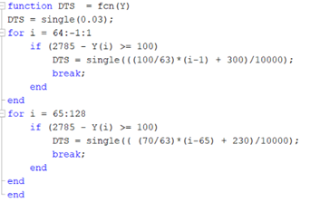 |
| Fig 23. Matlab function for computing the DTS |
3.4.4 Set The Servo
The DTS is then passed to another FTM_PWM_Config block to generate the signal needed to control the Servo.
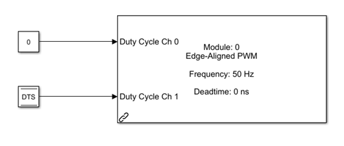 |
Fig 24. FTM block for controlling the servo
|
In order to do so, the block should be configured with the following parameters, which have the same signification as mentioned in chapter 3.4.1:
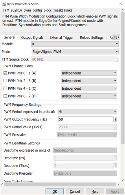 |
Fig 25. FTM block parameters |
According to the hardware connections from the S32K adapter board and the current setup, only one Servomotor is used, and this is the STEERINGPWM1 mentioned in the file with the mapping between the Landzo car pins and the S32K144 board. The allocated peripheral for this module is the FTM0_CH1, which means that the module 0 should be chosen from the configuration parameters together with the 0-1 pair of channels. To control the servo, only one signal is needed, so there is no need to use 2 channels. The complementary mode could have been used here, like in the camera CLK signal configuration, but doing so, only the configuration of channel 0 would have been possible and channel 1 is requested for the application. By choosing the independent mode, a duty cycle input will be available for the both channels of the pair, and because only channel 1 is needed for the control of this module, an input equal to 0 will be given to the other one. The frequency is set to 50Hz considering the motor construction particularities and a duty cycle equal to 0.03 (wheels not steered) is set as an initial value.
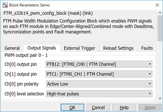 |
| Fig 26. FTM output signals |
3.4.5 Set The Motors
For the two rear motors, the same principle applies. The duty cycle (DT) is configured by default at the 0.1 value which will cause the car to move along the track with 10% of its maximum speed.
The frequency of the PWM signal that controls the motors is 5000Hz. This value is in the range specified in the datasheet of the motor drivers mentioned in the schematics.
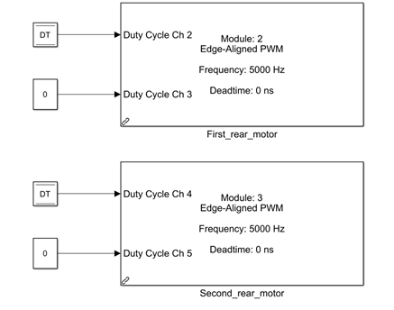 |
Fig 27. FTM block for controlling the traction motors |
For the control of a single motor, two signals are needed. The schematics of the Motor Driver board indicate that for the control of each motor two integrated circuits are used (BTN7960). They form an H bridge which looks as in the picture below.
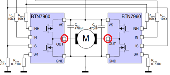 |
Fig 28. H bridge |
To make the motor spin, the potential difference of the points the motor is connected between must be different from 0. It can be observed that each integrated circuit needs an input signal. The pins that give the input signals to the circuits are corresponding to the output channels of the FTM block. Let’s take for example the 1st rear motor. It is controlled by a FTM Config block which outputs on the following channels.
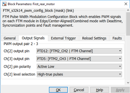 |
Fig 29. FTM output signals |
By setting and keeping channel 3 of the FTM Config block channels to 0, an input equal to 0 will be transmitted to one of the BTN modules as an input on the IN pin (for example, to the right one). This will trigger the right lower transistor to act like a closed switch. The transistor above it will remain opened, so the voltage of the OUT point will be 0V. The channel 2 corresponds to the other integrated circuit, and a positive input will be received by this one on the IN pin (left side of the picture). Now, the left upper transistor will act like a closed switch, and the one below will remain open, making the OUT point’s potential to represent a positive value (depending on the duty cycle given as an input to the FTM block). Thus, a potential difference is created and the motor will start spinning.
3.4.6 Configuration Block
In addition to all these, the model needs also a configuration block which is used to configure the target MCU, the compiler, the system clock frequency, etc. A configuration block is needed in all the models because it ensures the communication with the target.
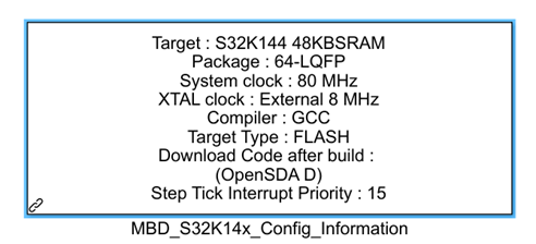 |
| Fig 30. Model configuration block |
The operation frequency can be chosen from the MCU tab of the block parameters window. For this model, it was set at 80Hz. The board model, the SRAM and the clock frequency can also be set from the MCU tab.
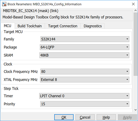 |
| Fig 31. Configuration block MCU tab |
If you want to change the compiler and also the optimization levels, click the Build Toolchain tab and take a look at the available options presented in the picture below. From this tab you can also choose the target memory for the model which can be FLASH or SRAM.
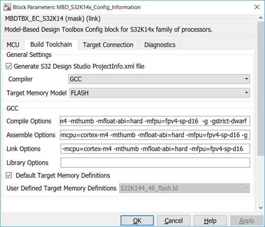 |
Fig 32. Configuration block Build Toolchain tab |
The application is downloaded on the target through OpenSDA. OpenSDA is an open standard serial and debug adapter. It bridges serial and debug communications between a USB host and an embedded target processor. Make sure that the Download Code after Build option is checked in order to see your application running on the target.
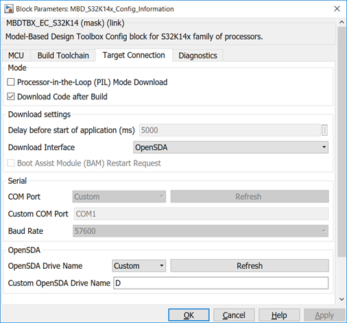 |
Fig 33. Configuration block Target Connection tab |
For additional information about the blocks used in this model, right-click on them and choose the ‘Help’ option available in the menu.
4. How To Debug The Application Using FreeMaster
In order to use FreeMaster for debugging and managing the information from your application, a FreeMaster configuration block must be used in the Simulink model.
 |
Fig 34. FreeMaster configuration block |
The block parameters should be configured as in the following picture:
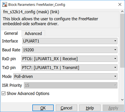 |
| Fig 35. FreeMaster configuration block parameters |
The interface field specifies the communication interface between the application and the FreeMaster. LPUART1 is chosen in this example because it is directly connected to the OpenSDA. OpenSDA is an open standard serial and debug adapter. It bridges serial and debug communications between a USB host and an embedded target processor. The BaudRate represents the speed of data transmission between the application and the FreeMaster and it is expressed in kbps. The receive data pin and the transmit data pin should be always configured to PTC6, respectively PTC7 (for the LPUART1 interface) because these pins are connected to the OpenSDA Receive and Transmit pins, as specified in the HMI Mapping.
 |
Fig 36. OpenSDA to LPUART1 connection |
By clicking the Show Advanced Options checkbox, multiple settings are available and their functionalities are all specified in the Help file which will open after clicking the Help button in the Block Parameters tab.
The variables that need to be observed changing over time must be declared Volatile. The variables already added to the FreeMaster project are declared using the Data Store Memory block.
 |
Fig 37. Global Variables |
The Volatile option can be chosen from the Block Parameters Tab. After double clicking the Data Store Memory block, click the Signal Attributes tab and in the Code Generation groupbox, set the Storage Class option to Volatile (Custom), as in the picture below.
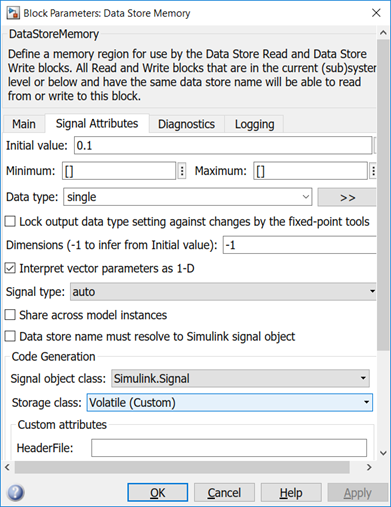 |
| Fig 38. Data store memory block parameters |
For calling the FreeMaster data acquisition each time a subsystem is triggered, a FreeMaster Recorder Call block should be added in the subsystem where the variables that you want to record are computed. Thus, a recorder block is placed in the subsystem which is triggered at 100us for recording the evolution of C and conv variables.
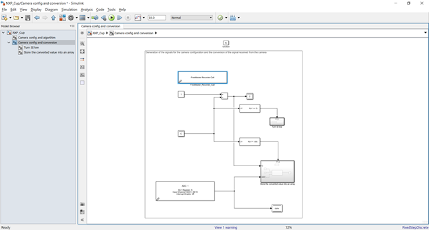 |
| Fig 39. FreeMaster recorder call |
To check the functionality of the FreeMASTER, open the .pmp file with the same name as the Simulink model and click on the red STOP button in order to initialize the communication with the S32K144 evaluation board.
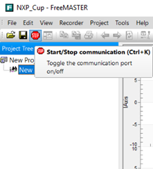 |
Fig 40. Start/Stop FreeMaster communication |
If errors appear, click on the Project menu and open the Options window. Make sure that the port value is the same as the one on which your S32K144 is connected (you can check the COM number of the evaluation board in the Device Manager window). Make sure also that the Speed is the same as the baud rate of the FreeMaster Config block.
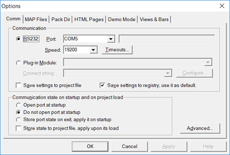 |
Fig 41. FreeMaster communication setup |
Click on the MAP Files tab and ensure that the default symbol file is the .elf file from the folder that is created when you build your Simulink model. It should be called (your_model_name.elf).
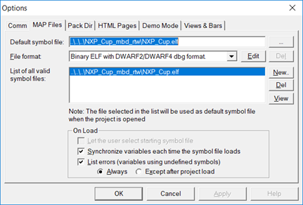 |
Fig 42. FreeMaster .elf file |
Once the connection is set and the app working, you will observe how the values of the variables in the Variable Watch are changing.
Click on the Recorder option from the left side of the window in order to see the graphical evolution of the variables.
You can add or remove variables from the watch by right-clicking inside the Variable Watch area and choosing the Watch Properties options.
Right clicking on the Recorder will provide a Properties option as well. Use that for selecting the variables that you want to display and for many other options.
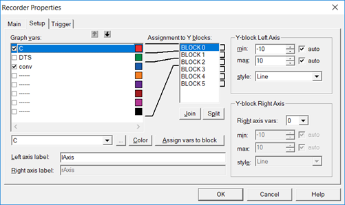 |
Fig 43. FreeMaster recorder properties |
5. Autonomous Intelligent Car Demonstration And Hints For Improvement
5.1 Demo
If you want to make sure that everything works as it is supposed to before actually putting the car on the track, you can use the FreeMaster tool to visualize the evolution of the variables of your project. Considering every setup was made as specified, here is what you should expect to see.
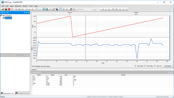 |
Fig 44. Variable Watch |
The two rear motors duty cycle and also the one for the camera CLK signal should have constant values all the time (0.1 respectively 0.5). The DTS should vary its values between 0.023 and 0.04 as mentioned in the Camera to Steer algorithm chapter. C variable must be incremented every 100us and reset every 20ms, this meaning that when it reaches 200, it should be set back at 0. This evolution can also be graphically observed by using the recorder option. Conv variable and Y array represent the conversion result and all the bottoms of the conv graphical evolution represent the existence of a dark color in the visual field of the car.
A demonstration video with the car following the track for a lap is attached to the current content.
5.2 Improvement Areas
The application proposed uses a basic if-else algorithm in order to compute the steering of the front wheels based on the track in front of the car. A proof of the concept that the vehicle can be controlled and kept on the path using a S32K144 board and a Model Based Design approach is realized in the presented solution. Major improvements regarding the lap time could be achieved by developing a way to control also the car speed which now is at a constant value. Many other hardware and software solutions can be designed and implemented with the purpose of obtaining the fastest autonomous self driving car for the NXP Cup.
| NXP CUP - LINE FOLLOWER WITH MODEL-BASED DESIGN TOOLBOX FOR S32K MICROPROCESSOR | ||
- Mark as Read
- Mark as New
- Bookmark
- Permalink
- Report Inappropriate Content
Hi, am5885712@gmail.com
Thank you for your feedback on the article :smileyhappy:
Sure, please feel free to ask me any questions on the topic.
Kind Regards,
Irina