- NXP Forums
- Product Forums
- General Purpose MicrocontrollersGeneral Purpose Microcontrollers
- i.MX Forumsi.MX Forums
- QorIQ Processing PlatformsQorIQ Processing Platforms
- Identification and SecurityIdentification and Security
- Power ManagementPower Management
- MCX Microcontrollers
- S32G
- S32K
- S32V
- MPC5xxx
- Other NXP Products
- Wireless Connectivity
- S12 / MagniV Microcontrollers
- Powertrain and Electrification Analog Drivers
- Sensors
- Vybrid Processors
- Digital Signal Controllers
- 8-bit Microcontrollers
- ColdFire/68K Microcontrollers and Processors
- PowerQUICC Processors
- OSBDM and TBDML
-
- Solution Forums
- Software Forums
- MCUXpresso Software and ToolsMCUXpresso Software and Tools
- CodeWarriorCodeWarrior
- MQX Software SolutionsMQX Software Solutions
- Model-Based Design Toolbox (MBDT)Model-Based Design Toolbox (MBDT)
- FreeMASTER
- eIQ Machine Learning Software
- Embedded Software and Tools Clinic
- S32 SDK
- S32 Design Studio
- Vigiles
- GUI Guider
- Zephyr Project
- Voice Technology
- Application Software Packs
- Secure Provisioning SDK (SPSDK)
- Processor Expert Software
-
- Topics
- Mobile Robotics - Drones and RoversMobile Robotics - Drones and Rovers
- NXP Training ContentNXP Training Content
- University ProgramsUniversity Programs
- Rapid IoT
- NXP Designs
- SafeAssure-Community
- OSS Security & Maintenance
- Using Our Community
-
- Cloud Lab Forums
-
- Home
- :
- Topics
- :
- NXP Designs
- :
- Re: The result of MHT2012N DC tracing simulation is quite different from data given by the datasheet
The result of MHT2012N DC tracing simulation is quite different from data given by the datasheet
- Subscribe to RSS Feed
- Mark Topic as New
- Mark Topic as Read
- Float this Topic for Current User
- Bookmark
- Subscribe
- Mute
- Printer Friendly Page
The result of MHT2012N DC tracing simulation is quite different from data given by the datasheet
- Mark as New
- Bookmark
- Subscribe
- Mute
- Subscribe to RSS Feed
- Permalink
- Report Inappropriate Content
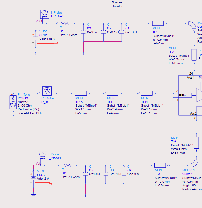
In order to design a power amplifier with MHT2012N,I use the DC tracing simulation in ADS with the ADS model,but the result is different from the data given by the datasheet.
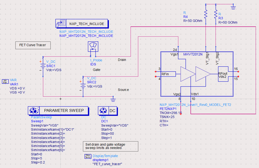
The schematic of DC tracing for the first stage
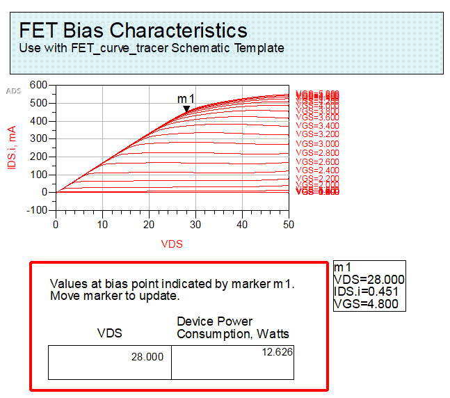
And the result
But according to the datasheet,if Vds=28V and Vgs=4.8V,Ids should be about 12mA which is much smaller than 451mA in the simlulation result.Why?
The second stage is the same.The simulation result is different from the data given by the datasheet.Can someone tell me the reason?Thank you very much!
- Mark as New
- Bookmark
- Subscribe
- Mute
- Subscribe to RSS Feed
- Permalink
- Report Inappropriate Content
below
- Mark as New
- Bookmark
- Subscribe
- Mute
- Subscribe to RSS Feed
- Permalink
- Report Inappropriate Content
1.
The simulation is correct. But, you misinterpret datasheet specs.
MHT2012N VGS1 is not a fan out pin of the isolated RF transistor gate. Indeed, the voltage at the gate is equal to VGS1. However, it is not a high impedance input. It also includes temperature compensation circuit that sinks current from the pin to GND.
https://www.nxp.com/docs/en/application-note/AN1977.pdf
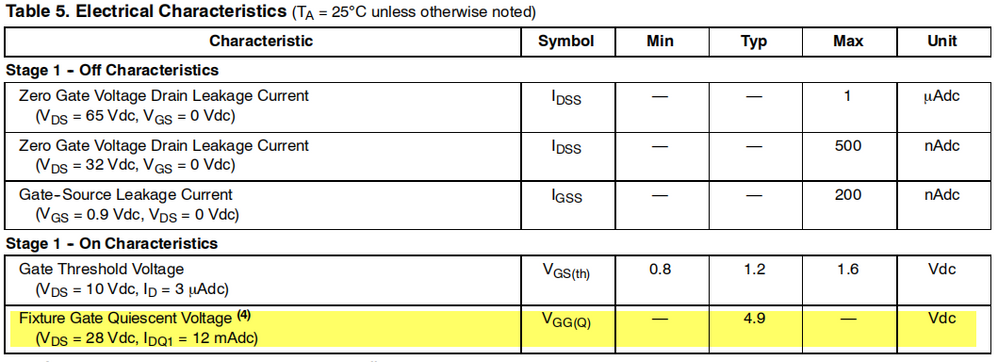
MHT2012N datasheet Table 4 "Stage 1 - On Characteristics" provides two parameters:
- VGS(th) gate threshold voltage ~1.2V @ ID=3uA
- Fixture Gate Quiescent Voltage ~4.9V @ ID=12mA
There is a note 4 "Data measured in NXP test fixture with 4.7 kOhm resistor in series with VGS1 and VGS2pins."
The first parameter is the voltage measured at the VGS1 pin. The second parameter is the voltage measured at the 4.7kOhm resistor that is sum of the voltage at the VGS1 pin plus the voltage drop at the resistor.
So, a current at this pin is (4.9V-1.2V)/4.7kOhm ~ 0.8mA (taking into account gate overvoltage, more accurate value is about 0.65mA).
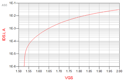
In your simulation, you swept VGS from 0V to 5V. More appropriate range is [1.5-2.0]V. The reference current 12mA is achieved at VGS1~1.85V.
2.
Unfortunately, the MHT2012N model PDK does not include clear description of the model. In fact, the kit does not include temperature compensation circuit and, thus, it doesn't sink the current. So, you can not simulate temperature compensation circuit using this model.
Nevertheless, this model provides correct ID current dependency vs VGS voltage. In practice, all you need is to tune the voltage at VGS1, VGS2 pins to obtain desired quiescent currents IDS1 and IDS2.
Best Regards
Pavel
NXP TIC
- Mark as New
- Bookmark
- Subscribe
- Mute
- Subscribe to RSS Feed
- Permalink
- Report Inappropriate Content
Thank you very much.
According to my simulation,the reference current IDQ1=12mA is achieved at VGS1~1.85V and IDQ2=72mA is achieved at VGS2~2V. In my simulation,if VGS1=1.85V and VGS2=2V(even both with 4.7kOhm resistor),the result is right(output about 41.8dBm and gain about 30dB).
However,in your reference circuit(I mean the evaluation board),it says that VGS1=VGS2=4.8V with a 4.7 kOhm resistor in series with VGS1 and VGS2.But in the simulation,if VGS1=VGS2=4.8V(both with 4.7kOhm resistor), everything goes wrong(output power is smaller than input power,gain<0dB).
All I want to know is that if the simulation does not agree with the circuit?Or does that mean if I tune VGS to a value in the simulation but in the circuit I need to change it to another value?Is it due to the lack of temperature compensation circuit of the PDK?
Thanks.
