- NXP Forums
- Product Forums
- General Purpose MicrocontrollersGeneral Purpose Microcontrollers
- i.MX Forumsi.MX Forums
- QorIQ Processing PlatformsQorIQ Processing Platforms
- Identification and SecurityIdentification and Security
- Power ManagementPower Management
- MCX Microcontrollers
- S32G
- S32K
- S32V
- MPC5xxx
- Other NXP Products
- Wireless Connectivity
- S12 / MagniV Microcontrollers
- Powertrain and Electrification Analog Drivers
- Sensors
- Vybrid Processors
- Digital Signal Controllers
- 8-bit Microcontrollers
- ColdFire/68K Microcontrollers and Processors
- PowerQUICC Processors
- OSBDM and TBDML
-
- Solution Forums
- Software Forums
- MCUXpresso Software and ToolsMCUXpresso Software and Tools
- CodeWarriorCodeWarrior
- MQX Software SolutionsMQX Software Solutions
- Model-Based Design Toolbox (MBDT)Model-Based Design Toolbox (MBDT)
- FreeMASTER
- eIQ Machine Learning Software
- Embedded Software and Tools Clinic
- S32 SDK
- S32 Design Studio
- Vigiles
- GUI Guider
- Zephyr Project
- Voice Technology
- Application Software Packs
- Secure Provisioning SDK (SPSDK)
- Processor Expert Software
-
- Topics
- Mobile Robotics - Drones and RoversMobile Robotics - Drones and Rovers
- NXP Training ContentNXP Training Content
- University ProgramsUniversity Programs
- Rapid IoT
- NXP Designs
- SafeAssure-Community
- OSS Security & Maintenance
- Using Our Community
-
-
- Home
- :
- Identification and Security
- :
- NFC
- :
- Re: When designing an NFC antenna on a PCB is it ok to have the antenna around the perimeter of the board and have components located in the center? What minimum spacing should be maintained between components and the antenna?
When designing an NFC antenna on a PCB is it ok to have the antenna around the perimeter of the board and have components located in the center? What minimum spacing should be maintained between components and the antenna?
- Subscribe to RSS Feed
- Mark Topic as New
- Mark Topic as Read
- Float this Topic for Current User
- Bookmark
- Subscribe
- Mute
- Printer Friendly Page
When designing an NFC antenna on a PCB is it ok to have the antenna around the perimeter of the board and have components located in the center? What minimum spacing should be maintained between components and the antenna?
- Mark as New
- Bookmark
- Subscribe
- Mute
- Subscribe to RSS Feed
- Permalink
- Report Inappropriate Content
I am designing a board that will have NFC capabilities and am wondering if it is ok to just have the antenna go around the outer perimeter of the board and have the components in the center?
- Mark as New
- Bookmark
- Subscribe
- Mute
- Subscribe to RSS Feed
- Permalink
- Report Inappropriate Content
Hi,
Having the componentes outside the antenna space is the best option, but if you have size constraints you can have components inside the antenna area. You need to follow these considerations:
- Avoid Magnetic loops in general (other than the antenna itself)
- Strong magnetic coupling between antenna and anything else
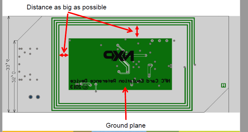
- Propert GND layer (area rather than single traces)
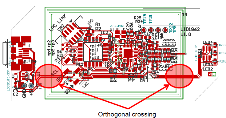
- Use orthogonal crossing of antenna traces and others (if required)
- Distance as big as possible between components and the antenna.
I recommend to check the specific NFC Reader antenna design guide. As example, you can see the PN5180 NFC Reader Antenna Design guide document https://www.nxp.com/docs/en/application-note/AN11740.pdf
Hope the information hepls,
Regards,
Adrian Cano
- Mark as New
- Bookmark
- Subscribe
- Mute
- Subscribe to RSS Feed
- Permalink
- Report Inappropriate Content
That's very useful information, thanks Adrian. Can I extend Nate's question and ask what clearance should be respected around the PCB antenna? I can't seem to find that information in the documentation you linked. I'm looking at a Class 1 type antenna.
Thanks,
- Felix -

