- Forums
- Product Forums
- General Purpose MicrocontrollersGeneral Purpose Microcontrollers
- i.MX Forumsi.MX Forums
- QorIQ Processing PlatformsQorIQ Processing Platforms
- Identification and SecurityIdentification and Security
- Power ManagementPower Management
- Wireless ConnectivityWireless Connectivity
- RFID / NFCRFID / NFC
- Advanced AnalogAdvanced Analog
- MCX Microcontrollers
- S32G
- S32K
- S32V
- MPC5xxx
- Other NXP Products
- S12 / MagniV Microcontrollers
- Powertrain and Electrification Analog Drivers
- Sensors
- Vybrid Processors
- Digital Signal Controllers
- 8-bit Microcontrollers
- ColdFire/68K Microcontrollers and Processors
- PowerQUICC Processors
- OSBDM and TBDML
- S32M
- S32Z/E
-
- Solution Forums
- Software Forums
- MCUXpresso Software and ToolsMCUXpresso Software and Tools
- CodeWarriorCodeWarrior
- MQX Software SolutionsMQX Software Solutions
- Model-Based Design Toolbox (MBDT)Model-Based Design Toolbox (MBDT)
- FreeMASTER
- eIQ Machine Learning Software
- Embedded Software and Tools Clinic
- S32 SDK
- S32 Design Studio
- GUI Guider
- Zephyr Project
- Voice Technology
- Application Software Packs
- Secure Provisioning SDK (SPSDK)
- Processor Expert Software
- Generative AI & LLMs
-
- Topics
- Mobile Robotics - Drones and RoversMobile Robotics - Drones and Rovers
- NXP Training ContentNXP Training Content
- University ProgramsUniversity Programs
- Rapid IoT
- NXP Designs
- SafeAssure-Community
- OSS Security & Maintenance
- Using Our Community
-
- Cloud Lab Forums
-
- Knowledge Bases
- ARM Microcontrollers
- i.MX Processors
- Identification and Security
- Model-Based Design Toolbox (MBDT)
- QorIQ Processing Platforms
- S32 Automotive Processing Platform
- Wireless Connectivity
- CodeWarrior
- MCUXpresso Suite of Software and Tools
- MQX Software Solutions
- RFID / NFC
- Advanced Analog
-
- NXP Tech Blogs
How to output pwm using DMA for MPC55xx/MPC56xx ?
Hi,
I did not see a demo using DMA for updating CADR/CBDR in PWM output modes. Maybe some code for input capture mode using DMA can be found.
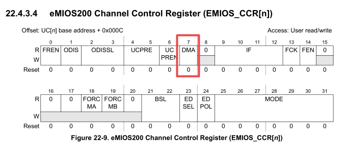
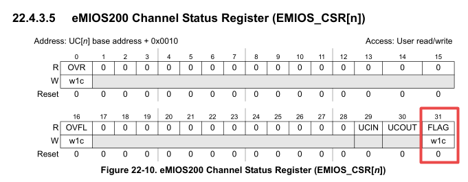
Anyway, if DMA bit is set, the FLAG generates DMA request. You can program the DMA channel to do what you need finally. If DMA bit is set the FLAG is cleared by DMA controller after DMA transfer is done.
I can recommend you to refer to AN2865 (https://www.nxp.com/docs/en/application-note/AN2865.pdf ). In this cookbook note you can find example for setting eMIOS output PWM mode as well as DMA codes. You can try to combine them together to achieve desired functionality on your MCU.
BR, Petr
Hi,I have tried to accomplish code follow your advice, but it can't ouput pwm waveform.
Could you tell me what the mistake is ??? Thank you !
void Dma_eMIOS_Init(void)
{
EDMA.CR.R = 0x0000000C;
SIU.PCR[179].B.PA = 1;
SIU.PCR[179].B.OBE = 1;
EMIOS.MCR.B.MDIS = 0;
EMIOS.MCR.B.GPRE = 3;
EMIOS.MCR.B.ETB = 0;
EMIOS.MCR.B.GTBE = 1;
EMIOS.MCR.B.FRZ = 1;
EMIOS.MCR.B.GPREN = 1;
// OPWFMB mode
EMIOS.CH[0].CCR.B.MODE = 0x58;
EMIOS.CH[0].CBDR.R = 1;
EMIOS.CH[0].CCR.B.BSL = 3;
EMIOS.CH[0].CCR.B.UCPREN = 1;
EMIOS.CH[0].CCR.B.UCPRE = 0;
EMIOS.CH[0].CCR.B.EDPOL = 0;
EMIOS.CH[0].CCR.B.FEN = 1;
EMIOS.CH[0].CCR.B.DMA = 1;
EMIOS.CH[0].CSR.B.FLAG = 1;
}
void eMIOS_DmaSetPeriodAndDuty(int *DutyAndPeriod)
{
// source address - duty and period array
EDMA.TCD[20].SADDR = (int)DutyAndPeriod;
// 32-bit
EDMA.TCD[20].SSIZE = 2;
// src addr increment 4 bytes
EDMA.TCD[20].SOFF = 4;
// after major loop, back to beginning
EDMA.TCD[20].SLAST = -(4 * 2);
// source modulo feature not used
EDMA.TCD[20].SMOD = 0;
// dest. address - Channel A Data Register
EDMA.TCD[20].DADDR = (int)&(EMIOS.CH[0].CADR.R);
// 32-bit
EDMA.TCD[20].DSIZE = 2;
// dest addr increment 4 bytes, the next register is Channel B Data Register (CBDR)
EDMA.TCD[20].DOFF = 4;
// after major loop, back to beginning
EDMA.TCD[20].DLAST_SGA = -(4 * 2);
EDMA.TCD[20].DMOD = 0;
// 4 byte per minor loop
EDMA.TCD[20].NBYTES = 4;
// 2 major iteration count
EDMA.TCD[20].BITER = 2;
EDMA.TCD[20].CITER = 2;
EDMA.TCD[20].CITERE_LINK = 0;
EDMA.TCD[20].BITERE_LINK = 0;
EDMA.TCD[20].MAJORE_LINK = 0;
EDMA.TCD[20].MAJORLINKCH = 0;
EDMA.TCD[20].D_REQ = 0;
EDMA.TCD[20].INT_HALF = 0;
EDMA.TCD[20].INT_MAJ = 0;
EDMA.TCD[20].E_SG = 0;
EDMA.TCD[20].BWC = 0;
EDMA.TCD[20].START = 0;
EDMA.TCD[20].DONE = 0;
EDMA.TCD[20].ACTIVE = 0;
// enable dma channel
EDMA.SERQR.R = 20;
}
void mian(void)
{
// duty=100, period=200
int t_duty_and_period[2] = {100, 200};
Dma_eMIOS_Init();
eMIOS_DmaSetPeriodAndDuty(t_duty_and_period);
for (;;);
}

