- NXP Forums
- Product Forums
- General Purpose MicrocontrollersGeneral Purpose Microcontrollers
- i.MX Forumsi.MX Forums
- QorIQ Processing PlatformsQorIQ Processing Platforms
- Identification and SecurityIdentification and Security
- Power ManagementPower Management
- MCX Microcontrollers
- S32G
- S32K
- S32V
- MPC5xxx
- Other NXP Products
- Wireless Connectivity
- S12 / MagniV Microcontrollers
- Powertrain and Electrification Analog Drivers
- Sensors
- Vybrid Processors
- Digital Signal Controllers
- 8-bit Microcontrollers
- ColdFire/68K Microcontrollers and Processors
- PowerQUICC Processors
- OSBDM and TBDML
-
- Solution Forums
- Software Forums
- MCUXpresso Software and ToolsMCUXpresso Software and Tools
- CodeWarriorCodeWarrior
- MQX Software SolutionsMQX Software Solutions
- Model-Based Design Toolbox (MBDT)Model-Based Design Toolbox (MBDT)
- FreeMASTER
- eIQ Machine Learning Software
- Embedded Software and Tools Clinic
- S32 SDK
- S32 Design Studio
- Vigiles
- GUI Guider
- Zephyr Project
- Voice Technology
- Application Software Packs
- Secure Provisioning SDK (SPSDK)
- Processor Expert Software
-
- Topics
- Mobile Robotics - Drones and RoversMobile Robotics - Drones and Rovers
- NXP Training ContentNXP Training Content
- University ProgramsUniversity Programs
- Rapid IoT
- NXP Designs
- SafeAssure-Community
- OSS Security & Maintenance
- Using Our Community
-
-
"Mini-Monkey" Part 2: Using MCUXpresso to Accelerate the PCB Design Process
"Mini-Monkey" Part 2: Using MCUXpresso to Accelerate the PCB Design Process
- Subscribe to RSS Feed
- Mark as New
- Mark as Read
- Bookmark
- Subscribe
- Printer Friendly Page
- Report Inappropriate Content
In part two in this series on designing with the LPC55S69 VFBGA98 package, I am going to show you how to use the NXP MCUXpresso SDK tools to help with physical design process. Combining some features in MCUXpresso with my PCB tool of choice, Altium Designer, I can significantly reduce the time in the CAD process.
The first step in designing a PCB with a new MCU is to add the part into your component libraries. Component library management can a source of passionate disagreements between design engineers. My own view on library management is rooted in many years of making mistakes! These simple mistakes ultimately caused delays and made projects more difficult than they needed to be. Often time these mistakes were also driven by a desire to "save time". Given my experience, there are a few overarching principles I adhere to.
- The individual making the component should also be the one who has to stay the weekend and cut traces if a mistake is made. This obviously conflicts of the “librarian/drafter” model but I literally have seen projects where the librarian made a mistake on a 1000+ pin BGA that cost >$5k. This model was put in a library and marked as “verified”. The person making the parts needs some skin in the game! In this case, the drafting teams claimed they had a processing that included a double check but *no one in that process knew they context on how the part was going to be used*.
- Pulling models from the internet or external libraries is OK as a starting point but it is just that, A starting point. You must treat every pin as if it was wrong and verify. Since many organizations have specific rules on how a part should look, you will need to massage the model to meet your own needs. Software engineers shake their head at this rule. "Why not build on somebody else's libraries? It is what we do!". Well, A mistake in a hardware library can take weeks if not months to really solve.... The cost, time and frustration impact can be huge. We hardware engineers can't simply "re-compile".
- I don’t trust any footprint unless I know it has been used in a successful design. The context of how a part is used is very important (which leads to #4).
- I believe the design re-used is best done at a schematic snippet level, not an individual part. After all, once I get this Mini-Monkey board complete, I will never again start with just the LPC55S69. I want all the “stuff” surrounding the chip that makes it work!
To the casual observer, these principles seems onerous and time consuming but I have found that the *save me time over the course of the project*. Making your own parts may seem time consuming but it *does not have to be*. There are tools that can make your life simpler and the task less arduous. Also making your own CAD part is useful for a few other reasons:
- You have to go through a mental exercise when looking at each of the pins. It forces you brain to think about functionality in a slightly different way. When starting with a new part/family, repeated exposure is a very good way to learn.
- Looking at the footprint early on gets your brain in a planning mode for when you do get started.
One could argue that this is “lost” time as compared to getting someone else to do the CAD library management it but I really feel strongly that it saves time in the long run. I have witnessed too many projects sink time into unnecessary debugging due to the bad CAD part creation. I feel the architect of the design needs to be intimately involved and take ownership of the process.
The LPC55S69 in the VFBGA package has only 98 pins. With no automation or tools, it would not take all that long build a part right from the datasheet. However, it is on the edge of being a time consuming endeavor. Also, when I build schematic symbols, I tend to label the pins with all possible IO capabilities allowed by the MCU pin mux. This can make the part quite large but it also helps see what also is available on a pin if I am in in a debug pinch. Creating pins with all this detail can be quite time consuming. I use Altium Designer for all of my PCB design and it has some useful automation to make parts more quickly. NXP’s MCUXpresso tool also has a unique feature that can really help board designers get work done quickly.
Creating the Pin List
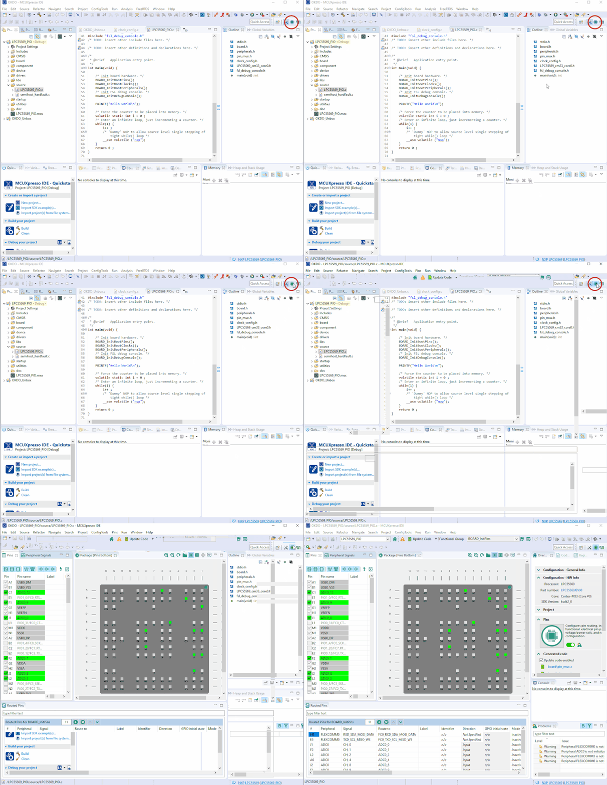
Built into MCUXpresso is a pins tool that is *very* useful in large projects with setting up the pin mux’s and doing some advanced planning. While it is primarily a tool for bootstrapping pin setup for the firmware, It can also use useful to drive the CAD part creation process. Simply create a new project and start the pins tool:
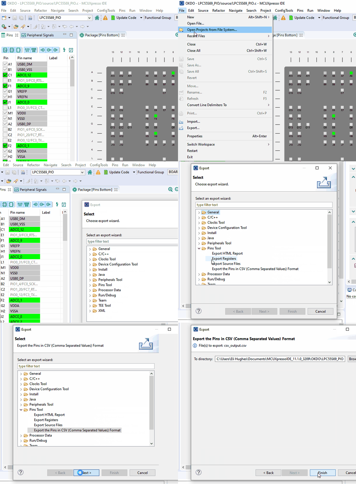
The pins tools gives you a tabular and physical view of pin assignments. Very useful when planning your PCB routing. We will use the export feature to get a list of all the pins, numbers and labels.
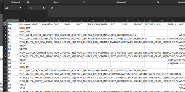
The pins tool generates a CSV file that you can bring into your favorite editor. Not only do I get the pin/ball numbers, I get all of the IO options available via the MCU pin mux.
Using the Pin List To Generate Component Pins
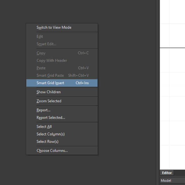
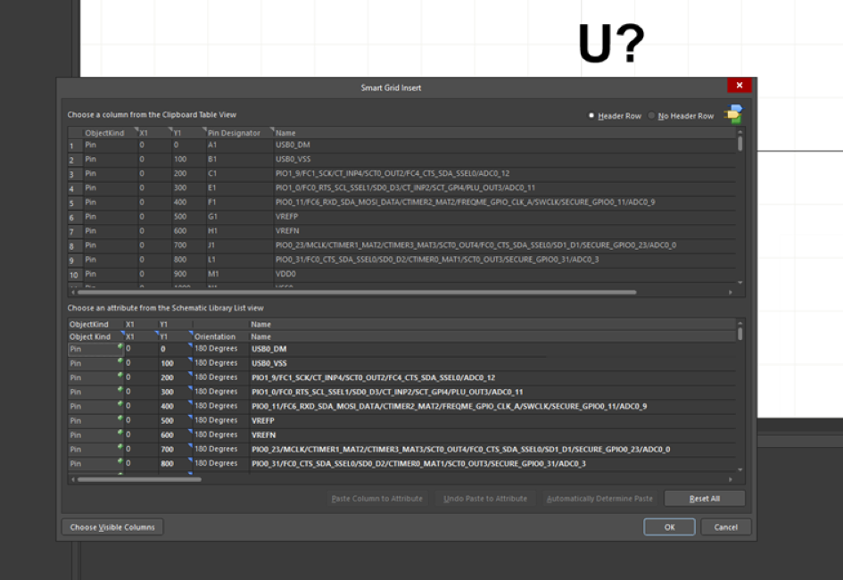
With just a few modifications, I can get the spreadsheet into a format useful for the Altium Smart Grid Paste Tool.
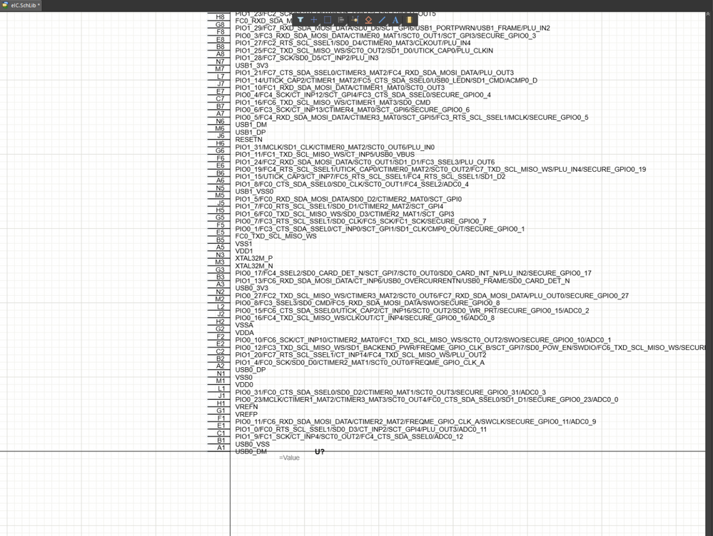
Altium Designer requires a few extra columns of meta-data to be able import the data into a grouping of pins in the schematic library editor. At this point you could group the pins to your personal preference. I personally like to see all pin function of the schematic but does create rather large symbols. The good news here is that by using MCUXpresso and Altium you can make this a 10-minute job, not a 3 hour one. Imagine going through the reference manual line by line!
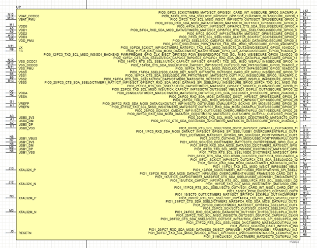
Viola! A complete symbol. It just took a few minutes of massaging to get what I wanted. Like I stated previously, a 98 pin package is not that bad to do manually but you can imagine a 200 or 300 pin part (such as the i.MX RT!)
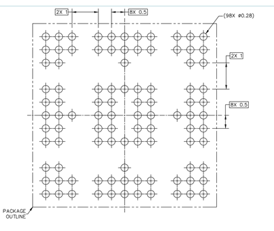
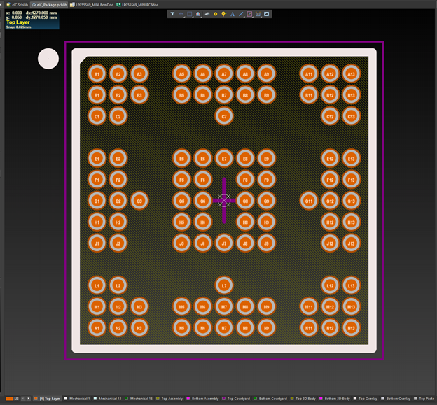
The VFBGA package is 7mmx7mm with a 0.5mm pitch. There are balls removed from the grid for easier route escaping when use this part with lower cost fabrication processes.
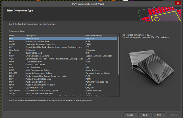
Once again, with a quick look at NXP documentation and using the Altium IPC footprint generator, we can make quick work of getting an accurate footprint.
The IPC footprint generator steps you through the entire process. All you need is the reference drawing.
A quick note about the IPC footprint tool in this use case. The NXP VFBGA has quite a few balls removed to allow of easier escaping. The IPC footprint generator can automatically remove certain regions, I found that this particular arrangement needed a few minutes of hand work to delete the unneeded pads given the unique pattern.
By using Altium and NXP’s MCUXpresso tool together, I was about to get my CAD library work done very quickly. And because I spent some time with the design tools, I became more familiar with the IO’s and physical package. This really helps get the brain primed for the real design work.
At this point in the proces I have a head start on the schematic entry and PCB layout. Next time we are going to dive in a bit to see what connections we need to bootstrap the LPC55S69 to get it up and running. We will take a look at some of the core components to get the MCU to boot and some peripheral functions that will help the Mini-Monkey come alive!
You must be a registered user to add a comment. If you've already registered, sign in. Otherwise, register and sign in.
-
101
6 -
communication standards
4 -
General Purpose Microcontrollers
19 -
i.MX RT Processors
45 -
i.MX Processors
43 -
introduction
9 -
LPC Microcontrollers
73 -
MCUXpresso
32 -
MCUXpresso Secure Provisioning Tool
1 -
MCUXpresso Conig Tools
30 -
MCUXpresso IDE
40 -
MCUXpresso SDK
25 -
Model-Based Design Toolbox
6 -
MQX Software Solutions
2 -
QorIQ Processing Platforms
1 -
QorIQ Devices
5 -
S32N Processors
4 -
S32Z|E Processors
6 -
SW | Downloads
4
- « Previous
- Next »
