- Forums
- Product Forums
- General Purpose MicrocontrollersGeneral Purpose Microcontrollers
- i.MX Forumsi.MX Forums
- QorIQ Processing PlatformsQorIQ Processing Platforms
- Identification and SecurityIdentification and Security
- Power ManagementPower Management
- Wireless ConnectivityWireless Connectivity
- RFID / NFCRFID / NFC
- Advanced AnalogAdvanced Analog
- MCX Microcontrollers
- S32G
- S32K
- S32V
- MPC5xxx
- Other NXP Products
- S12 / MagniV Microcontrollers
- Powertrain and Electrification Analog Drivers
- Sensors
- Vybrid Processors
- Digital Signal Controllers
- 8-bit Microcontrollers
- ColdFire/68K Microcontrollers and Processors
- PowerQUICC Processors
- OSBDM and TBDML
- S32M
- S32Z/E
-
- Solution Forums
- Software Forums
- MCUXpresso Software and ToolsMCUXpresso Software and Tools
- CodeWarriorCodeWarrior
- MQX Software SolutionsMQX Software Solutions
- Model-Based Design Toolbox (MBDT)Model-Based Design Toolbox (MBDT)
- FreeMASTER
- eIQ Machine Learning Software
- Embedded Software and Tools Clinic
- S32 SDK
- S32 Design Studio
- GUI Guider
- Zephyr Project
- Voice Technology
- Application Software Packs
- Secure Provisioning SDK (SPSDK)
- Processor Expert Software
- Generative AI & LLMs
-
- Topics
- Mobile Robotics - Drones and RoversMobile Robotics - Drones and Rovers
- NXP Training ContentNXP Training Content
- University ProgramsUniversity Programs
- Rapid IoT
- NXP Designs
- SafeAssure-Community
- OSS Security & Maintenance
- Using Our Community
-
- Cloud Lab Forums
-
- Knowledge Bases
- ARM Microcontrollers
- i.MX Processors
- Identification and Security
- Model-Based Design Toolbox (MBDT)
- QorIQ Processing Platforms
- S32 Automotive Processing Platform
- Wireless Connectivity
- CodeWarrior
- MCUXpresso Suite of Software and Tools
- MQX Software Solutions
- RFID / NFC
- Advanced Analog
-
- NXP Tech Blogs
- Home
- :
- General Purpose Microcontrollers
- :
- LPC Microcontrollers
- :
- Problem in LPC18xx User Manual
Problem in LPC18xx User Manual
- Subscribe to RSS Feed
- Mark Topic as New
- Mark Topic as Read
- Float this Topic for Current User
- Bookmark
- Subscribe
- Mute
- Printer Friendly Page
- Mark as New
- Bookmark
- Subscribe
- Mute
- Subscribe to RSS Feed
- Permalink
- Report Inappropriate Content
Hi!
I have found an inconsistency in the User Manual for a LPC1857 (UM10430 Rev 3.0).
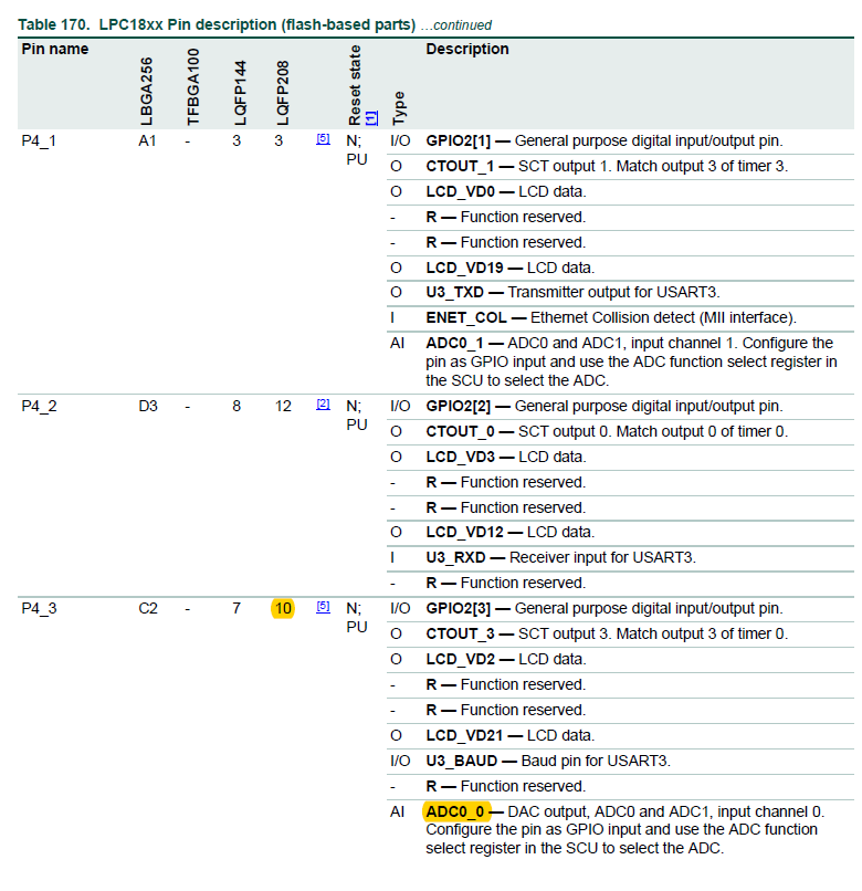
In p292 it says:
- ADC0_0 in P4_3::LQFP208::pin 10
- ADC0_1 en P4_1::LQFP208::pin 3
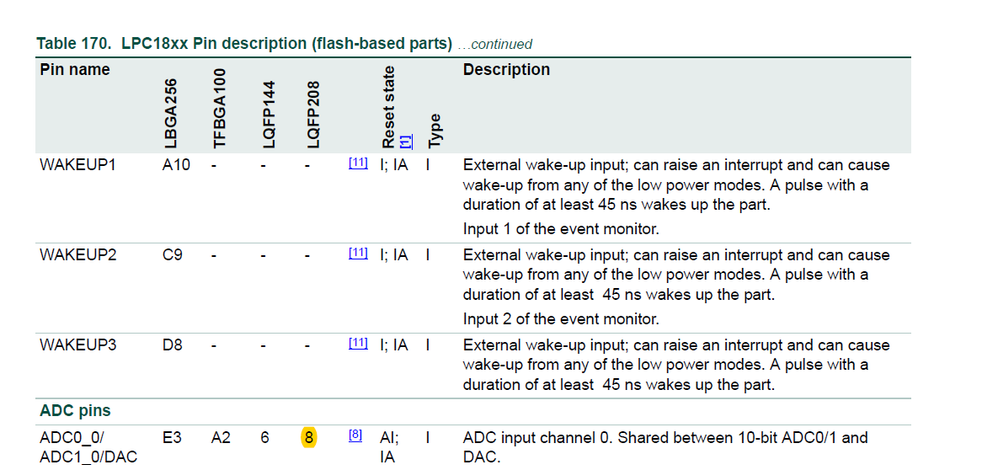
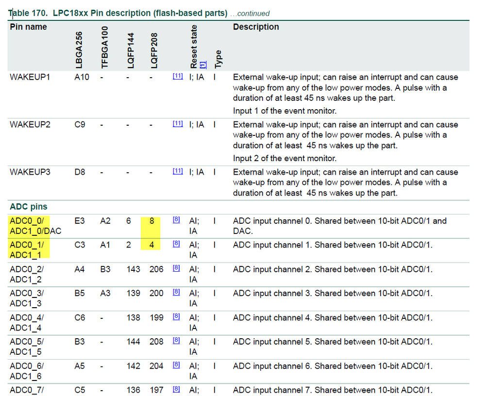
Then in p328 it says:
- ADC0_0 en LQFP208::pin 8
- ADC0_1 en LQFP208::pin 4
I have a board made to an altium design, and in the altium symbol the ADC pins are as described in p328. But then I cannot read ADC values in those pins. I have not checked the rest of the channels, my design uses only those two. I have a workaround in my board, I have to solder jumper wires to use channels 3 and 4.
Could you please look into the matter and correct the UM? I haven't found a newer UM or any errata about this.
Best regards!
Alex
Solved! Go to Solution.
- Mark as New
- Bookmark
- Subscribe
- Mute
- Subscribe to RSS Feed
- Permalink
- Report Inappropriate Content
Hi Alejandro Celery,
You have explained yourself very well in the first post, I got what you mean.
Still take ADC0_0 as an example, just as I told you, in LQFP208, both pin 8 and pin 10 can be used as ADC0_0 pin.
pin 10, P4_3 pin is the multi function pin, it can be work in both digital and analog mode, but pin 8, it is just the analog pin.
If you use pin8, you can use it as ADC0_0 directly, but if you use pin 10, you still need to configure this pin as the analog function, and choose it as the ADC pin.
So, actually, you can rout it to both pin 10 or pin 8, but if your digital pin is not enough, I suggest you use pin8, because pin 10 still can be used other digital function.
Wish this explain helps your understanding.
If you still have questions about this topic, please kindly let me know!
Have a great day,
Kerry
-----------------------------------------------------------------------------------------------------------------------
Note: If this post answers your question, please click the Correct Answer button. Thank you!
-----------------------------------------------------------------------------------------------------------------------
- Mark as New
- Bookmark
- Subscribe
- Mute
- Subscribe to RSS Feed
- Permalink
- Report Inappropriate Content
Hi Alejandro Celery,
Page p292 and p328 is not the inconsistency, it means you can use both P4_3 ,P4_1 and ADC0_0, ADC0_1.
P4_3 and P4_1 can be configured to ADC function or other digital function.
Both P292 and P328 should work. P4_3 and P4_1 also need to control SCU, configure it as the analog function in ENAIO0.
But, to p328 ,
These two pins(ADC0_0 and ADC0_1) should work when you just configure the ADC0.
Actually, even ADC0_3 and ADC0_4 also have the Port pin, ADC0_3 is P7_5, ADC0_4 is P7_4.
I am afraid you still need to check the ADC0_0 and ADC0_1 hardware solder and code.
Have a great day,
Kerry
-----------------------------------------------------------------------------------------------------------------------
Note: If this post answers your question, please click the Correct Answer button. Thank you!
-----------------------------------------------------------------------------------------------------------------------
- Mark as New
- Bookmark
- Subscribe
- Mute
- Subscribe to RSS Feed
- Permalink
- Report Inappropriate Content
Hi Kerry!
It seems like I have not explained myself well.
Let's take just one pin to make it easier to explain the problem, ADC0_0.
If I look at page 292 of the UM, it says that ADC0_0 is on pin number 10
(ten) of the LQFP 208 package.
If I look at page 328 of the UM, it says that ADC0_0 is on pin number 8
(eight) of the LQFP 208 package.
So when routing the board, I wouldn't know in which pin of the LQFP 208
package is the ADC0_0 pin.
Please let me know if I have explained myself better.
Thanks!
Saludos,
Alejandro
El 23/10/17 a las 01:37, kerryzhou escribió:
>
NXP Community
<https://community.freescale.com/resources/statics/1000/35400-NXP-Community-Email-banner-600x75.jpg>
>
Re: Problem in LPC18xx User Manual
reply from Kerry Zhou
<https://community.nxp.com/people/kerryzhou?et=watches.email.thread>
in /LPC/ - View the full discussion
<https://community.nxp.com/message/954244?commentID=954244&et=watches.email.thread#comment-954244>
>
- Mark as New
- Bookmark
- Subscribe
- Mute
- Subscribe to RSS Feed
- Permalink
- Report Inappropriate Content
Hi Alejandro Celery,
You have explained yourself very well in the first post, I got what you mean.
Still take ADC0_0 as an example, just as I told you, in LQFP208, both pin 8 and pin 10 can be used as ADC0_0 pin.
pin 10, P4_3 pin is the multi function pin, it can be work in both digital and analog mode, but pin 8, it is just the analog pin.
If you use pin8, you can use it as ADC0_0 directly, but if you use pin 10, you still need to configure this pin as the analog function, and choose it as the ADC pin.
So, actually, you can rout it to both pin 10 or pin 8, but if your digital pin is not enough, I suggest you use pin8, because pin 10 still can be used other digital function.
Wish this explain helps your understanding.
If you still have questions about this topic, please kindly let me know!
Have a great day,
Kerry
-----------------------------------------------------------------------------------------------------------------------
Note: If this post answers your question, please click the Correct Answer button. Thank you!
-----------------------------------------------------------------------------------------------------------------------
- Mark as New
- Bookmark
- Subscribe
- Mute
- Subscribe to RSS Feed
- Permalink
- Report Inappropriate Content
Hi Kerry!
Now I unsterstand and I was able to fix my problem. Thank you very much for your explanation.
At the time I felt that the User Manual was not clear enough on the subject, maybe you can make it better on a next release.
Thanks for your time!
Regards,
Alex


