- NXP Forums
- Product Forums
- General Purpose MicrocontrollersGeneral Purpose Microcontrollers
- i.MX Forumsi.MX Forums
- QorIQ Processing PlatformsQorIQ Processing Platforms
- Identification and SecurityIdentification and Security
- Power ManagementPower Management
- MCX Microcontrollers
- S32G
- S32K
- S32V
- MPC5xxx
- Other NXP Products
- Wireless Connectivity
- S12 / MagniV Microcontrollers
- Powertrain and Electrification Analog Drivers
- Sensors
- Vybrid Processors
- Digital Signal Controllers
- 8-bit Microcontrollers
- ColdFire/68K Microcontrollers and Processors
- PowerQUICC Processors
- OSBDM and TBDML
-
- Solution Forums
- Software Forums
- MCUXpresso Software and ToolsMCUXpresso Software and Tools
- CodeWarriorCodeWarrior
- MQX Software SolutionsMQX Software Solutions
- Model-Based Design Toolbox (MBDT)Model-Based Design Toolbox (MBDT)
- FreeMASTER
- eIQ Machine Learning Software
- Embedded Software and Tools Clinic
- S32 SDK
- S32 Design Studio
- Vigiles
- GUI Guider
- Zephyr Project
- Voice Technology
- Application Software Packs
- Secure Provisioning SDK (SPSDK)
- Processor Expert Software
-
- Topics
- Mobile Robotics - Drones and RoversMobile Robotics - Drones and Rovers
- NXP Training ContentNXP Training Content
- University ProgramsUniversity Programs
- Rapid IoT
- NXP Designs
- SafeAssure-Community
- OSS Security & Maintenance
- Using Our Community
-
-
- Home
- :
- 通用微控制器
- :
- LPC微控制器知识库
- :
- [LPC55xx] :Power Supply Circuit Design and Detection Method
[LPC55xx] :Power Supply Circuit Design and Detection Method
[LPC55xx] :Power Supply Circuit Design and Detection Method
[LPC55xx] :Power Supply Circuit Design and Detection Method
1. Problem description
When we debug a new designed LPC55 custom board through SWD, if IDE throws out error messages such as connection failure or no available device being found, normally we must check below two points:
- Whether the debug circuit design is correct.(https://community.nxp.com/t5/LPCXpresso-IDE-FAQs/Design-Considerations-for-Debug/m-p/469565#M44)
- Whether LPC55 power supply system is correct.
Regarding to the second point of power supply system, we received many feedback from customers that even they read UM for times they still can’t well-understand LPC55xx DCDC power supply system. Therefore we prepare this article to analyze LPC55xx power supply circuit and introduce detection method.
2. Problem Analysis
The difference of power supply circuit between LPC55xx series and other LPCs is that LPC55xx uses DCDC circuit inside to provide core voltage. It lowers the input 1.8V-3.6V voltage to around 1.1V to supply LPC55xx internal system. The DCDC converter is efficient and reduces the internal power consumption. The disadvantage is that it generates a certain ripple.
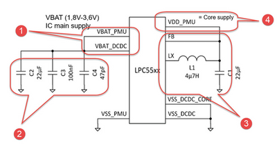
LPC55xx power supply circuit is as follows:

In order to analyze, We divide LPC55xx power supply circuit into 4 regions and will introduce them one by one according to the different functions.
1) Input voltage: In this part, VBAT_PMU provides input voltage to RTC and internal analog components. VBAT_DCDC provides input voltage to internal DCDC circuit.
2) A set of filter capacitors: To filter out the burrs and glitch at the voltage input.
3) DCDC circuit: Work with LPC55xx internal DCDC circuit together to generate 1.1V output voltage.
4) VDD_PMU: Provides the 1.1V output voltage of the DCDC circuit to the LPC55xx core.
Note: The design of region 3 is to work with the internal DCDC converter. The inductance L1 of 4μ7H and the capacitance C1 of 22μF are calculated by LPC55xx internal circuit. When designing, we must strictly follow the parameters recommended in the manual, otherwise DCDC circuit can’t work normally.
3. DCDC Circuit Detection
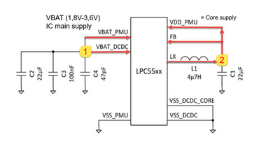
LPC55xx power supply system current direction is shown in the diagram below. See arrow in red. In order to ensure the normal operation of the DCDC circuit, the following two detection points are recommended.

1) Detection point 1: External 1.8 to 3.6V voltage input, normally it’s 3.3V.
2) Detection point 2: Output of the DCDC converter. If the DCDC works normally, we can get 1.1V voltage output here. The output voltage supplies power to the core components such as the central processing unit through the VDD_PMU.
If DCDC convert input is correct but output wrong, we suggest checking inductor L1 and the capacitor C1 and related solder issue. If the voltage of two detection points are correct, the power supply circuit problem can be ruled out.
4. summary:
For custom designed LPC55xx board, if SWD design is correct and power supply system works well, IDE can connect, download and debug target without issue.
