- NXP Forums
- Product Forums
- General Purpose MicrocontrollersGeneral Purpose Microcontrollers
- i.MX Forumsi.MX Forums
- QorIQ Processing PlatformsQorIQ Processing Platforms
- Identification and SecurityIdentification and Security
- Power ManagementPower Management
- MCX Microcontrollers
- S32G
- S32K
- S32V
- MPC5xxx
- Other NXP Products
- Wireless Connectivity
- S12 / MagniV Microcontrollers
- Powertrain and Electrification Analog Drivers
- Sensors
- Vybrid Processors
- Digital Signal Controllers
- 8-bit Microcontrollers
- ColdFire/68K Microcontrollers and Processors
- PowerQUICC Processors
- OSBDM and TBDML
-
- Solution Forums
- Software Forums
- MCUXpresso Software and ToolsMCUXpresso Software and Tools
- CodeWarriorCodeWarrior
- MQX Software SolutionsMQX Software Solutions
- Model-Based Design Toolbox (MBDT)Model-Based Design Toolbox (MBDT)
- FreeMASTER
- eIQ Machine Learning Software
- Embedded Software and Tools Clinic
- S32 SDK
- S32 Design Studio
- Vigiles
- GUI Guider
- Zephyr Project
- Voice Technology
- Application Software Packs
- Secure Provisioning SDK (SPSDK)
- Processor Expert Software
-
- Topics
- Mobile Robotics - Drones and RoversMobile Robotics - Drones and Rovers
- NXP Training ContentNXP Training Content
- University ProgramsUniversity Programs
- Rapid IoT
- NXP Designs
- SafeAssure-Community
- OSS Security & Maintenance
- Using Our Community
-
-
- Home
- :
- 通用微控制器
- :
- Kinetis微控制器
- :
- SWD in KL03
SWD in KL03
Hello,
It's right this connection in order to program the KL03 32kb QFN-24 with the LPC_Link_v2 ?
With 3 wires, DIO, CLK and RESET because I can not put a SWD standard connector because I have not space.
BR
已解决! 转到解答。
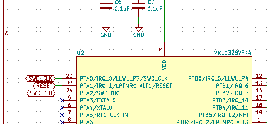
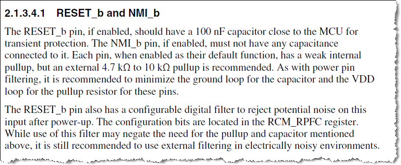
NMI_b(PTB5) external pullup resistor
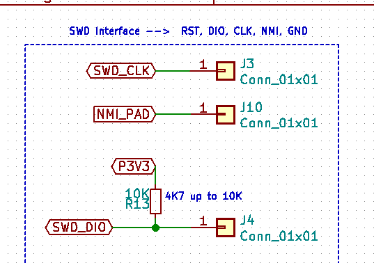
SWD_DIO(PTA2) external pullup resistor
SWD_CLK(PTA0)
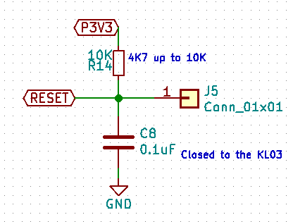
RESET_b(PTA1) external pullup resistor / 100 nF capacitor
GND is needed when using LPC_Link_v2 connect to KL03.
Best Regards,
Robin
-----------------------------------------------------------------------------------------------------------------------
Note: If this post answers your question, please click the Correct Answer button. Thank you!
-----------------------------------------------------------------------------------------------------------------------
Thank you!,
Then, it's ok so?
SWD_DIO
RESET
Is the capacitor well connected? It's a 100nF 0402 ceramic capacitor.
NMI
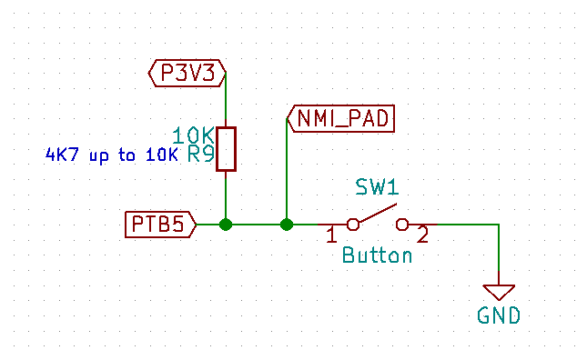
I had already NMI pull-up 10K resistor and one button in order to enter in boot mode. It's necessary the NMI pad for use the LCP_Link2? It's enought with the button? I can remove it?
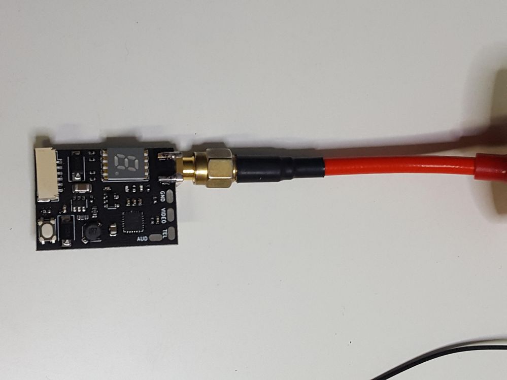
SW1 the only button I have on the pcb. I plan to use it to change channels/bands and to enter boot mode.
Best regards
Hello,
I'm try to programmer the KL03 with the LPC-Link2 but I get this error (in linux):
Executing flash operation 'Erase' (Erase flash) - Tue May 07 23:40:33 WEST 2019
Checking MCU info...
Scanning for targets...
Executing flash action...
MCUXpresso IDE RedlinkMulti Driver v10.3 (Nov 28 2018 02:37:04 - crt_emu_cm_redlink build 748)
( 0) Reading remote configuration
Wc(03). No cache support.
Found part description in XML file MKL03Z4_internal.xml
( 5) Remote configuration complete
Reconnected to existing link server
redlink server client - failed to receive response (to op 26) from server after 2000ms - Connection timed out (rc 110)
Connecting to probe 1 core 0 (using server started externally) gave 'Ee(42). Could not connect to core.'
Connecting to probe 1 core 0 (using server started externally) gave 'Ee(42). Could not connect to core.'
Connecting to probe 1 core 0 (using server started externally) gave 'Ee(42). Could not connect to core.'
Server OK but no connection to probe 1 core 0 (after 3 attempts) - Ee(42). Could not connect to core.
Failed on connect: Ee(42). Could not connect to core.
No connection to chip's debug port
(100) Target Connection Failed
Unable to perform operation!
Command failed with exit code 1The wiring is so to the ARM Jtag 10 pins:
MKL03 - LPC-Link2
Reset PTA1 - Pin 10 RESET (10K 1%)
SWD_CLK PTA0 - Pin 4 TCLK
SWD_DIO PTA2 - Pin 2 TMS (10K 1%)
GND - Pin 3
On the board the button is connected to the PTB5 NMI (pullup with 10K 1%) of the MKL03

