- Forums
- Product Forums
- General Purpose MicrocontrollersGeneral Purpose Microcontrollers
- i.MX Forumsi.MX Forums
- QorIQ Processing PlatformsQorIQ Processing Platforms
- Identification and SecurityIdentification and Security
- Power ManagementPower Management
- Wireless ConnectivityWireless Connectivity
- RFID / NFCRFID / NFC
- Advanced AnalogAdvanced Analog
- MCX Microcontrollers
- S32G
- S32K
- S32V
- MPC5xxx
- Other NXP Products
- S12 / MagniV Microcontrollers
- Powertrain and Electrification Analog Drivers
- Sensors
- Vybrid Processors
- Digital Signal Controllers
- 8-bit Microcontrollers
- ColdFire/68K Microcontrollers and Processors
- PowerQUICC Processors
- OSBDM and TBDML
- S32M
- S32Z/E
-
- Solution Forums
- Software Forums
- MCUXpresso Software and ToolsMCUXpresso Software and Tools
- CodeWarriorCodeWarrior
- MQX Software SolutionsMQX Software Solutions
- Model-Based Design Toolbox (MBDT)Model-Based Design Toolbox (MBDT)
- FreeMASTER
- eIQ Machine Learning Software
- Embedded Software and Tools Clinic
- S32 SDK
- S32 Design Studio
- GUI Guider
- Zephyr Project
- Voice Technology
- Application Software Packs
- Secure Provisioning SDK (SPSDK)
- Processor Expert Software
- Generative AI & LLMs
-
- Topics
- Mobile Robotics - Drones and RoversMobile Robotics - Drones and Rovers
- NXP Training ContentNXP Training Content
- University ProgramsUniversity Programs
- Rapid IoT
- NXP Designs
- SafeAssure-Community
- OSS Security & Maintenance
- Using Our Community
-
- Cloud Lab Forums
-
- Knowledge Bases
- ARM Microcontrollers
- i.MX Processors
- Identification and Security
- Model-Based Design Toolbox (MBDT)
- QorIQ Processing Platforms
- S32 Automotive Processing Platform
- Wireless Connectivity
- CodeWarrior
- MCUXpresso Suite of Software and Tools
- MQX Software Solutions
- RFID / NFC
- Advanced Analog
-
- NXP Tech Blogs
- Home
- :
- 汎用マイクロコントローラ
- :
- Kinetisマイクロコントローラ
- :
- How to use the MK64FN1M0VLL12
How to use the MK64FN1M0VLL12
- RSS フィードを購読する
- トピックを新着としてマーク
- トピックを既読としてマーク
- このトピックを現在のユーザーにフロートします
- ブックマーク
- 購読
- ミュート
- 印刷用ページ
- 新着としてマーク
- ブックマーク
- 購読
- ミュート
- RSS フィードを購読する
- ハイライト
- 印刷
- 不適切なコンテンツを報告
Hello.
I have been verified using MK64FN1M0VLL12.
It connects to the following pin, but it does not work. The will it or not missing something?
Crystal frequency is confirmed with an oscilloscope.
[MCU]
13(VERGIN) -> 5.0v
22(VDDA) -> 3.3v
23(VREFH) -> 3.3v
24(VREFL) -> Gnd
25(VSSA) -> Gnd
28(XTAL32) -> 25MHz quartz crystal unit
29(EXTAL32)-> 25MHz quartz crystal unit
30(VBAT) -> 3.3v
34(PTA0) -> SWD_4 PIN
37(PTA3) -> SWD_2 PIN
50(PTA18) -> 50Mhz quartz crystal unit
51(PTA19) -> Gnd
52(RESET_b)-> SWD_10_PIN
68(PTB22) -> LED
74(VDD) -> 3.3v
75(VSS) -> Gnd
It should be noted that the program is already written over the SWD.
Using scheduled for LED test the 68(PTB22)PIN.
解決済! 解決策の投稿を見る。
- 新着としてマーク
- ブックマーク
- 購読
- ミュート
- RSS フィードを購読する
- ハイライト
- 印刷
- 不適切なコンテンツを報告
Have you try to place bypass capacitors close to the VDD and VSS pins on the traces leading to the MCU?
Usually we connect all of the VDD pins to 3.3v.(Not only one pair of VDD and VSS)
If you didn't need USB module. Please connect VREGIN and VOUT33 together and tie to ground through a 10kΩ resistor. Do not tie directly to ground, as this causes a latch-up risk.
Best Regards,
Robin
- 新着としてマーク
- ブックマーク
- 購読
- ミュート
- RSS フィードを購読する
- ハイライト
- 印刷
- 不適切なコンテンツを報告
Connect all the VDD and VSS, was stable operation was established a capacitor!
Problem was solved with more. Thank you really received long correspondence.
Thank you, Robin
- 新着としてマーク
- ブックマーク
- 購読
- ミュート
- RSS フィードを購読する
- ハイライト
- 印刷
- 不適切なコンテンツを報告
I'm going to create your own board.
Chip who use a FRDM-K64F is the same board for comparison.
What I've tried are as follows.
Connection in the SWD has take the confirmation.
This was confirmed in the following way.
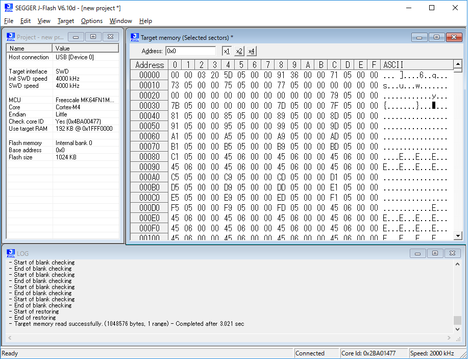
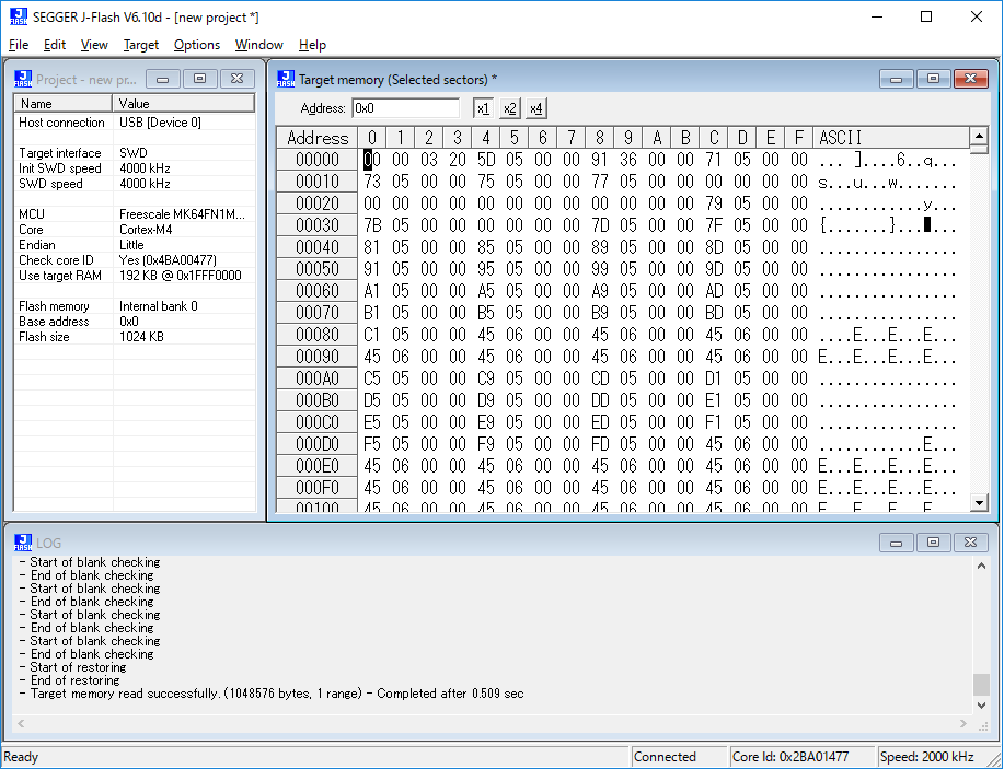
SEGGER J-Flash V6.10d of Target -> intended binary Read back was displayed.
Comparison is reading the same binary written in FRDM-K64F, were compared.
A binary that works with FRDM-K64F, when written in its own board, it has problems that do not work.
If I was to start the custom board in keil debug mode, you can see that the move rare. Procedure at that time was as follows.
Debug -> Start/Stop Debug Session -> Run -> Reset CPU -> Stop -> Run
- 新着としてマーク
- ブックマーク
- 購読
- ミュート
- RSS フィードを購読する
- ハイライト
- 印刷
- 不適切なコンテンツを報告
Have you try to place bypass capacitors close to the VDD and VSS pins on the traces leading to the MCU?
Usually we connect all of the VDD pins to 3.3v.(Not only one pair of VDD and VSS)
If you didn't need USB module. Please connect VREGIN and VOUT33 together and tie to ground through a 10kΩ resistor. Do not tie directly to ground, as this causes a latch-up risk.
Best Regards,
Robin
- 新着としてマーク
- ブックマーク
- 購読
- ミュート
- RSS フィードを購読する
- ハイライト
- 印刷
- 不適切なコンテンツを報告
What failure did you see when trying to use your custom board with MK64? Does it fail when you try to use SWD for connection? Or you were able to load code into MK64 flash but it does not run correctly?
Hao
- 新着としてマーク
- ブックマーク
- 購読
- ミュート
- RSS フィードを購読する
- ハイライト
- 印刷
- 不適切なコンテンツを報告
I've understood that the boot loader is unnecessary.
Where in the accompanying me binaries to confirm the action, we work with FRDM-K64F board. However, it did not work with mk64fn1m0vll12.
Because of the LED of the test, to compile the following projects in keil uvision v5.21.1.0, it was executed.
Freescale\TWR-K64F120M\Blinky\
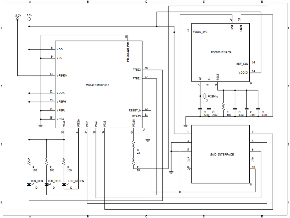
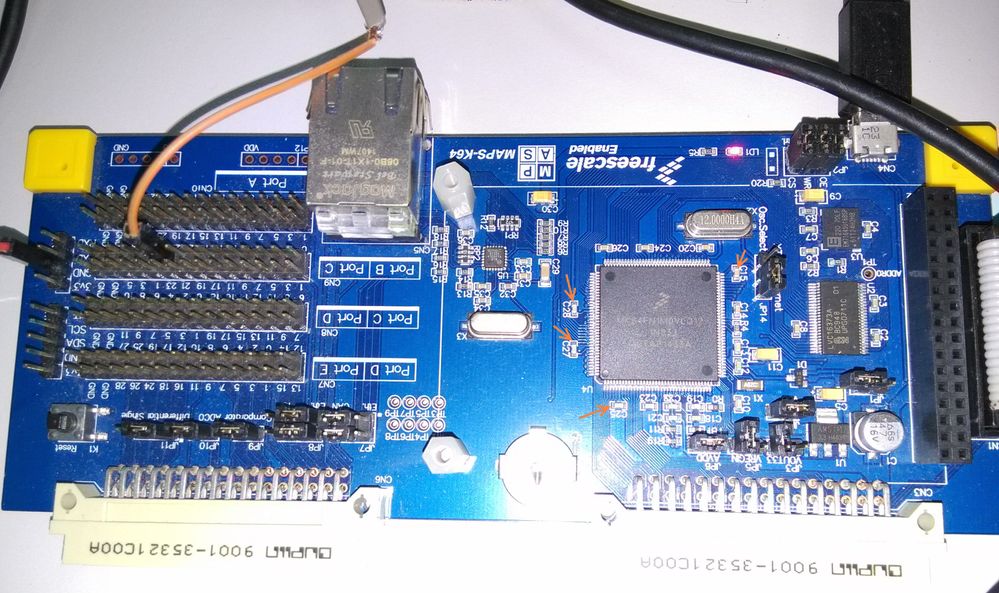
My to create a circuit I believe than there is a problem.
And, Circuit diagram is as follows.
- 新着としてマーク
- ブックマーク
- 購読
- ミュート
- RSS フィードを購読する
- ハイライト
- 印刷
- 不適切なコンテンツを報告
It is an additional question.
If the software is written in swd, but I think the boot loader is that it is unnecessary, incorrect?
- 新着としてマーク
- ブックマーク
- 購読
- ミュート
- RSS フィードを購読する
- ハイライト
- 印刷
- 不適切なコンテンツを報告
If the software is written in swd, the boot loader is unnecessary.
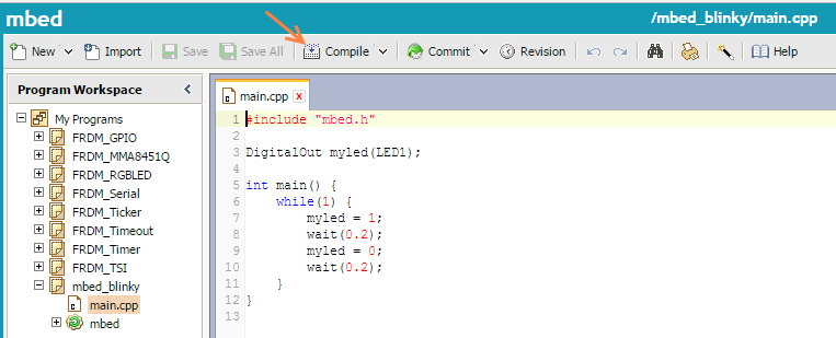
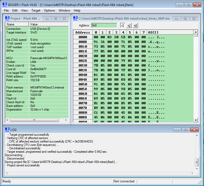
After compiled the mbed_blinky project, I got the mbed_blinky_K64F.bin file.
Writing of program uses the SEGGER J-Flash V4.92.
The PTB22 is toggle on my customer board.
Would you please attach the schematic here? So that we can check the circuit whether it has problem or not.
From your image, I can't see any bypass capacitors or resistors.
Supply routing – For Quad Flat Pack (QFP) packages, the power supply pins may be supplied radially to the MCU using traces rather than from planes. While it is adequate to place the bypass capacitors close to the VDD and VSS pins on the traces leading to the MCU, it is better to have the ground side of the bypass capacitor tied to the ground plane (through a via and short trace) close to the VSS pin and the VDD side tied to the power plane (through a via and short trace) close to the VDD pin.
Best Regards,
Robin
- 新着としてマーク
- ブックマーク
- 購読
- ミュート
- RSS フィードを購読する
- ハイライト
- 印刷
- 不適切なコンテンツを報告
Hi
Please observe the waveform of Reset_b with an oscilloscope. Make sure it high.( not sawtooth wave)
Please confirm the PTA4(NMI_b) is high. If the NMI input is low and the NMI function is enabled in the NMI_DIS field(by default), this results in an NMI interrupt.
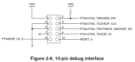
The RESET_b pin, if enabled, must have a 100 nF capacitor close to the MCU for transient protection. The NMI_b pin, if enabled, must not have any capacitance connected to it. Each pin, when enabled as their default function, has a weak internal pullup, but an external 4.7 kΩ to 10 kΩ pullup is recommended. As with power pin filtering, it is recommended to minimize the ground loop for the capacitor and the VDD loop for the pullup resistor for these pins.
The JTAG_TMS signal on PTA3 requires a strong pullup resistor for mode selection. For the debug interface, you can refer below image:
Do not connect 25MHz quartz crystal unit to RTC oscillator(XTAL32 and EXTAL32).
Best Regards,
Robin
- 新着としてマーク
- ブックマーク
- 購読
- ミュート
- RSS フィードを購読する
- ハイライト
- 印刷
- 不適切なコンテンツを報告
Thank you for your reply.
It was checked Reset_b, frequency of 50mhz was able to confirm.
In addition, it can be confirmed that it is the High, the waveform is also normal.
PTA4 was confirmed, was confirmed to be a High of 3.3v.
Crystal of 25Mhz was removed.
- 新着としてマーク
- ブックマーク
- 購読
- ミュート
- RSS フィードを購読する
- ハイライト
- 印刷
- 不適切なコンテンツを報告
I test the led_output project on my FRDM-K64F board. After download the program by using on board debugger, the LED RED is taking turns to shine.
If you download the Kinetis SDK2.0 for K64, the project can be found in below folder.(SDK_2.0_FRDM-K64F\boards\frdmk64f\driver_examples\gpio\led_output)
Would you please tell me what IDE are you using?(IAR or Keil MDK or KDS)
If you test the project on your own board, please attached the schematic here. So that we can check the circuit whether it has problem or not.
Do you mean that the project can't toggle the RED LED when debugging or normal run?
Best Regards,
Robin
- 新着としてマーク
- ブックマーク
- 購読
- ミュート
- RSS フィードを購読する
- ハイライト
- 印刷
- 不適切なコンテンツを報告
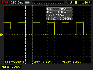
Operation check has been taken in the FRDM-K64F.
Compilation is doing in the online.
Development Platform for Devices | mbed
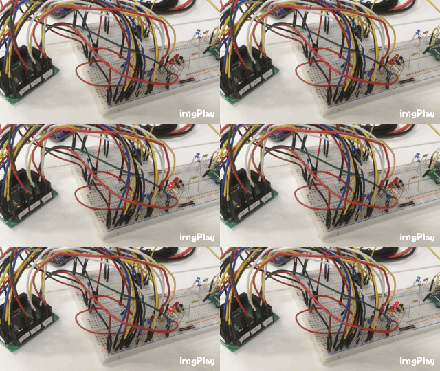
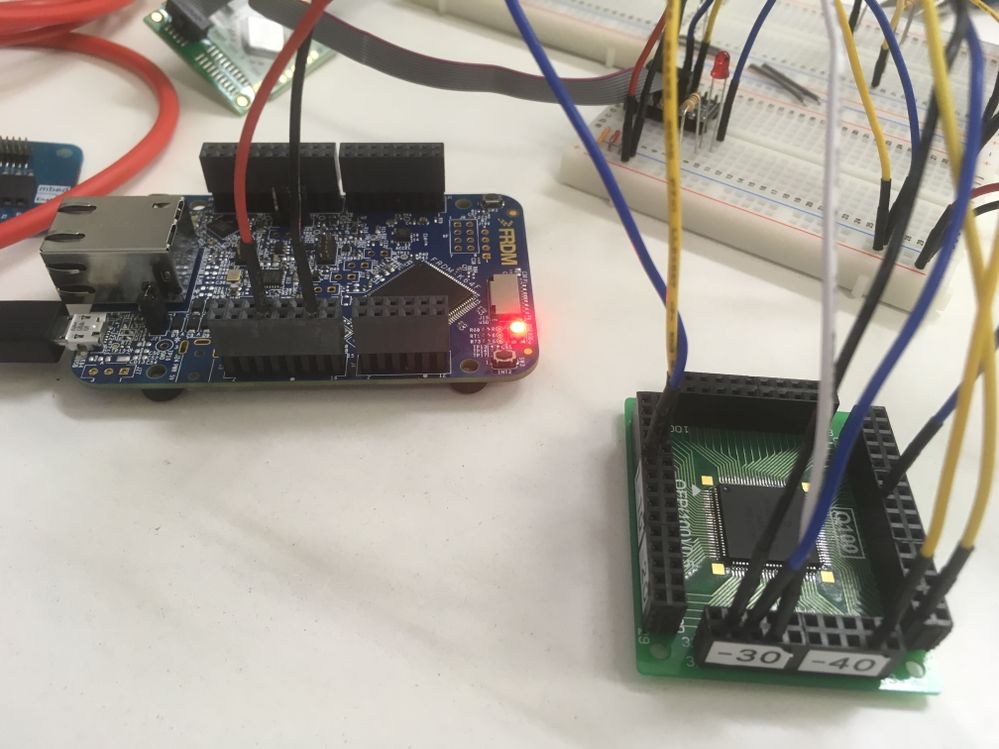
The following image is a thing of when the LED Blink test was carried out in FRDM-K64F.
Writing of program uses the SEGGER J-Flash V6.10d.
The program was considered to be funny, but it works fine in FRDM-K64F. For this reason, I thought whether the circuit is wrong.
