
- Forums
- Product Forums
- General Purpose MicrocontrollersGeneral Purpose Microcontrollers
- i.MX Forumsi.MX Forums
- QorIQ Processing PlatformsQorIQ Processing Platforms
- Identification and SecurityIdentification and Security
- Power ManagementPower Management
- Wireless ConnectivityWireless Connectivity
- RFID / NFCRFID / NFC
- Advanced AnalogAdvanced Analog
- Neural Processing UnitsNeural Processing Units
- MCX Microcontrollers
- S32G
- S32K
- S32V
- MPC5xxx
- Other NXP Products
- S12 / MagniV Microcontrollers
- Powertrain and Electrification Analog Drivers
- Sensors
- Vybrid Processors
- Digital Signal Controllers
- 8-bit Microcontrollers
- ColdFire/68K Microcontrollers and Processors
- PowerQUICC Processors
- OSBDM and TBDML
- S32M
- S32Z/E
-
- Solution Forums
- Software Forums
- MCUXpresso Software and ToolsMCUXpresso Software and Tools
- CodeWarriorCodeWarrior
- MQX Software SolutionsMQX Software Solutions
- Model-Based Design Toolbox (MBDT)Model-Based Design Toolbox (MBDT)
- FreeMASTER
- eIQ Machine Learning Software
- Embedded Software and Tools Clinic
- S32 SDK
- S32 Design Studio
- GUI Guider
- Zephyr Project
- Voice Technology
- Application Software Packs
- Secure Provisioning SDK (SPSDK)
- Processor Expert Software
- Generative AI & LLMs
-
- Topics
- Mobile Robotics - Drones and RoversMobile Robotics - Drones and Rovers
- NXP Training ContentNXP Training Content
- University ProgramsUniversity Programs
- Rapid IoT
- NXP Designs
- SafeAssure-Community
- OSS Security & Maintenance
- Using Our Community
-
- Cloud Lab Forums
-
- Knowledge Bases
- ARM Microcontrollers
- i.MX Processors
- Identification and Security
- Model-Based Design Toolbox (MBDT)
- QorIQ Processing Platforms
- S32 Automotive Processing Platform
- Wireless Connectivity
- CodeWarrior
- MCUXpresso Suite of Software and Tools
- MQX Software Solutions
- RFID / NFC
- Advanced Analog
- Neural Processing Units
-
- NXP Tech Blogs
- Home
- :
- 汎用マイクロコントローラ
- :
- Kinetisマイクロコントローラ
- :
- Re: How to program a kl03 board using SWD
How to program a kl03 board using SWD
- RSS フィードを購読する
- トピックを新着としてマーク
- トピックを既読としてマーク
- このトピックを現在のユーザーにフロートします
- ブックマーク
- 購読
- ミュート
- 印刷用ページ
How to program a kl03 board using SWD
- 新着としてマーク
- ブックマーク
- 購読
- ミュート
- RSS フィードを購読する
- ハイライト
- 印刷
- 不適切なコンテンツを報告
Hi everybody,
I'm developing a board based on the MCU KL03 that It would be able to be programmed by SWD connector and P&E Multilink Universal, but it doesn't work and it gives me this error:
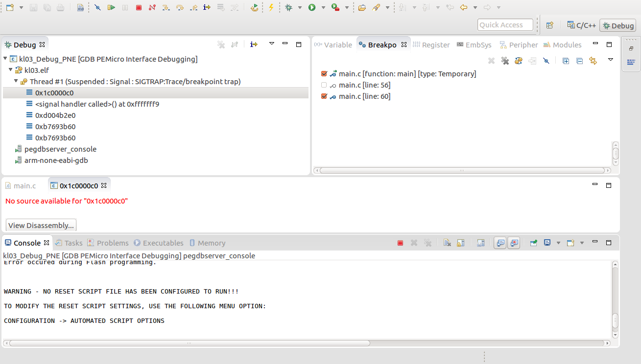
Erasing.
Module could not be erased.
Error Erasing flash of device
Error occured during Flash programming.
WARNING - NO RESET SCRIPT FILE HAS BEEN CONFIGURED TO RUN!!!
TO MODIFY THE RESET SCRIPT SETTINGS, USE THE FOLLOWING MENU OPTION:
CONFIGURATION -> AUTOMATED SCRIPT OPTIONS
PE-ERROR: Error downloading to the device.
I can't find the error. I have just control the whole circuit many times because I take out the five needed pins ( VCC, GND, Reset, SWD_CLK, SWD_DIO) that are welded on a male SWD.
Below there are the circuit.
- 新着としてマーク
- ブックマーク
- 購読
- ミュート
- RSS フィードを購読する
- ハイライト
- 印刷
- 不適切なコンテンツを報告
Hi Gianluca,
The schematic picture which you are attached is really very unclear.
Now, please check these points on your side:
1. SWD_DIO add 10K external pullup resistor
2. NMI pin add 4.7K to 10k external pullup resistor
3. Reset_b pin add 4.7K to 10k external pullup resistor, and a 0.1uf capacitor to ground.
4. SWD_CLK don't need to add external resistor.
6. Did you connect the correct wire sequence to the PE multilink, if the wire sequence is not correct, the chip won't be programmed.
7, chip solder temperature, the max data is 260°C. Don't be very higher, otherwise the chip maybe damaged.
Wish it helps you!
If you still have question, please let me know!
Have a great day,
Kerry
-----------------------------------------------------------------------------------------------------------------------
Note: If this post answers your question, please click the Correct Answer button. Thank you!
-----------------------------------------------------------------------------------------------------------------------
- 新着としてマーク
- ブックマーク
- 購読
- ミュート
- RSS フィードを購読する
- ハイライト
- 印刷
- 不適切なコンテンツを報告
Hi,
thank you for your answer! I have checked everything and I missed only the second point. What is it the external pull up resistor on NMI pin?
Have a great day.
Gianluca
- 新着としてマーク
- ブックマーク
- 購読
- ミュート
- RSS フィードを購読する
- ハイライト
- 印刷
- 不適切なコンテンツを報告
Hi Gianluca,
Because the NMI internal pullup is weak, it is better to add the external 4.7K to 10K pullup resistor in this pin.
You can use a 10K resistor between NMI pin and VDD.
Please try it on your side.
Any question, just let me know!
Have a great day,
Kerry
-----------------------------------------------------------------------------------------------------------------------
Note: If this post answers your question, please click the Correct Answer button. Thank you!
-----------------------------------------------------------------------------------------------------------------------
- 新着としてマーク
- ブックマーク
- 購読
- ミュート
- RSS フィードを購読する
- ハイライト
- 印刷
- 不適切なコンテンツを報告
Hi Kerry,
thank you for your suggestion and information. Unfortunately it doesn't work. I think is for either the soldering method or the SWD adptator. I'm thinking about another PCB more simple than this.
Thank you.
Have a great day.
Gianluca.
- 新着としてマーク
- ブックマーク
- 購読
- ミュート
- RSS フィードを購読する
- ハイライト
- 印刷
- 不適切なコンテンツを報告
Hi Gianluca,
Your Schematic picture is really not clear, I can't check it, please give me a more clear picture.
You must make sure the SWD wire sequence is correctly connected to the P&E multilink tool.
The following picture is from P&E multilink:

If you are using PORT G, please check the wire, is that correct to your mcu pin?
Wish it helps you!
If you still have question, please let me know!
Have a great day,
Jingjing
-----------------------------------------------------------------------------------------------------------------------
Note: If this post answers your question, please click the Correct Answer button. Thank you!
-----------------------------------------------------------------------------------------------------------------------