- Forums
- Product Forums
- General Purpose MicrocontrollersGeneral Purpose Microcontrollers
- i.MX Forumsi.MX Forums
- QorIQ Processing PlatformsQorIQ Processing Platforms
- Identification and SecurityIdentification and Security
- Power ManagementPower Management
- Wireless ConnectivityWireless Connectivity
- RFID / NFCRFID / NFC
- Advanced AnalogAdvanced Analog
- MCX Microcontrollers
- S32G
- S32K
- S32V
- MPC5xxx
- Other NXP Products
- S12 / MagniV Microcontrollers
- Powertrain and Electrification Analog Drivers
- Sensors
- Vybrid Processors
- Digital Signal Controllers
- 8-bit Microcontrollers
- ColdFire/68K Microcontrollers and Processors
- PowerQUICC Processors
- OSBDM and TBDML
- S32M
- S32Z/E
-
- Solution Forums
- Software Forums
- MCUXpresso Software and ToolsMCUXpresso Software and Tools
- CodeWarriorCodeWarrior
- MQX Software SolutionsMQX Software Solutions
- Model-Based Design Toolbox (MBDT)Model-Based Design Toolbox (MBDT)
- FreeMASTER
- eIQ Machine Learning Software
- Embedded Software and Tools Clinic
- S32 SDK
- S32 Design Studio
- GUI Guider
- Zephyr Project
- Voice Technology
- Application Software Packs
- Secure Provisioning SDK (SPSDK)
- Processor Expert Software
- Generative AI & LLMs
-
- Topics
- Mobile Robotics - Drones and RoversMobile Robotics - Drones and Rovers
- NXP Training ContentNXP Training Content
- University ProgramsUniversity Programs
- Rapid IoT
- NXP Designs
- SafeAssure-Community
- OSS Security & Maintenance
- Using Our Community
-
- Cloud Lab Forums
-
- Knowledge Bases
- ARM Microcontrollers
- i.MX Processors
- Identification and Security
- Model-Based Design Toolbox (MBDT)
- QorIQ Processing Platforms
- S32 Automotive Processing Platform
- Wireless Connectivity
- CodeWarrior
- MCUXpresso Suite of Software and Tools
- MQX Software Solutions
- RFID / NFC
- Advanced Analog
-
- NXP Tech Blogs
- Home
- :
- 通用微控制器
- :
- Kinetis微控制器
- :
- Engineering clock for FRDM-KE02Z40M
Engineering clock for FRDM-KE02Z40M
Engineering clock for FRDM-KE02Z40M
Hi NXP Community,
I have the FRDM-KE02Z40M board that has a 10MHz crystal. What is the engineering clock frequency for this uC? Usually this is derived from the crystal's frequency, for other MCU boards that I have worked with. I need this frequency for my timing subroutines, like a 20ms timing subroutine.
Thanks
Hi Circuit Man,
I think that you are making reference to the Core clock frequency.
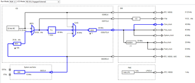
According the KE02 RM chapter 20 internal clock source, the internal clock is selected, since FLL Engaged Internal mode is automatically selected out of reset. Using MCUXpresso Config tools (Clocks Tool) and after selecting this FLL mode I have obtained 32 MHz of core clock frequency.
If you are using the MCUxpresso SDK, after running the BOARD_InitBootClocks(); the MCU is running with internal clock mode in FEE mode , core clock is 40 MHz.
However, I recommend you use the fsl_clock API, to determine any clock frequency from several IP's, including the Clock frequency.
uint32_t CLOCK_GetFreq(clock_name_t clockName);
This can be an easier way to determine clock values, for your delay API.
Additionally , If you are interested in Config tools, You can check our trainning videos and documentation, this tools helps users to initialize peripherals and clocks using a graphic interface.
And as a final recommendation, you can check out PIT timer demo in the KE02 SDK , for example, you can use the PIT timer to gererate delays. Our PIT API uses the clock frequency to calculate timings.
I hope this helps,
Diego.
Hi Diego,
Thank you for your response. I appreciate your help. But I have a question about your answer below. If the crystal's frequency is 10MHz, how can the KE02 core clock run at 40MHz? Doesn't the crystal set the maximum frequency of operation for the uC?
Thanks.
Hi @Circuit_Man
Thank you for your reply!
The internal FLL (frequency lock loop) generates a 40 MHz Core clock frequency by multiplying a reference clock by 1024, that way we are able to operate the MCU at a higher frequency than the one generated by the 10 MHz oscilator.
There are lots of documentation on the web detailing the operation of FLL´s and PLL´s. To complement my reply a bit more, besides the information in the RM you could look at the following application notes:
AN4757Migration Guide Chatpter 6 Clock modules from S08 to Kinetis E Family Clock modules.
If you like, you can also look at this application note https://www.nxp.com/docs/en/application-note/AN3041.pdf#page=3 where the FLL operation for the oldschool HCS08 MCU is described briefly.
I hope this could help you!
Yours,
Diego

