- NXP Forums
- Product Forums
- General Purpose MicrocontrollersGeneral Purpose Microcontrollers
- i.MX Forumsi.MX Forums
- QorIQ Processing PlatformsQorIQ Processing Platforms
- Identification and SecurityIdentification and Security
- Power ManagementPower Management
- MCX Microcontrollers
- S32G
- S32K
- S32V
- MPC5xxx
- Other NXP Products
- Wireless Connectivity
- S12 / MagniV Microcontrollers
- Powertrain and Electrification Analog Drivers
- Sensors
- Vybrid Processors
- Digital Signal Controllers
- 8-bit Microcontrollers
- ColdFire/68K Microcontrollers and Processors
- PowerQUICC Processors
- OSBDM and TBDML
-
- Solution Forums
- Software Forums
- MCUXpresso Software and ToolsMCUXpresso Software and Tools
- CodeWarriorCodeWarrior
- MQX Software SolutionsMQX Software Solutions
- Model-Based Design Toolbox (MBDT)Model-Based Design Toolbox (MBDT)
- FreeMASTER
- eIQ Machine Learning Software
- Embedded Software and Tools Clinic
- S32 SDK
- S32 Design Studio
- Vigiles
- GUI Guider
- Zephyr Project
- Voice Technology
- Application Software Packs
- Secure Provisioning SDK (SPSDK)
- Processor Expert Software
-
- Topics
- Mobile Robotics - Drones and RoversMobile Robotics - Drones and Rovers
- NXP Training ContentNXP Training Content
- University ProgramsUniversity Programs
- Rapid IoT
- NXP Designs
- SafeAssure-Community
- OSS Security & Maintenance
- Using Our Community
-
-
- Home
- :
- General Purpose Microcontrollers
- :
- Kinetis Microcontrollers
- :
- Re: Correctly calculate K8x QSPI SFA1AD, SFA2AD, SFB1AD and SFB2AD Register values.
Correctly calculate K8x QSPI SFA1AD, SFA2AD, SFB1AD and SFB2AD Register values.
- Subscribe to RSS Feed
- Mark Topic as New
- Mark Topic as Read
- Float this Topic for Current User
- Bookmark
- Subscribe
- Mute
- Printer Friendly Page
Correctly calculate K8x QSPI SFA1AD, SFA2AD, SFB1AD and SFB2AD Register values.
- Mark as New
- Bookmark
- Subscribe
- Mute
- Subscribe to RSS Feed
- Permalink
- Report Inappropriate Content
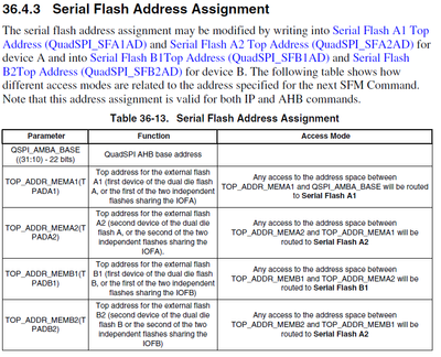
Does anyone know how to determine the correct settings for the K8x QSPI registers
QSPI_SFA1AD
QSPI_SFA2AD
QSPI_SFB1AD
QSPI_SFB2AD
Given the following QSPI Flash possibilities:
- (Dual) 2 x 64MB
- (Dual) 2 x 32MB
- (Single) 1 x 32MB
I really cannot get a satisfactory result using the documentation.
It's clear from this that the K8x QSPI can manage two dual-die chips, for a total of 4 dies. Our board uses only a single chip, which can be either a single- or dual-die.
For example, starting with simplest case, a single 32MB die connected as Serial Flash A1. The top address should be QSPI_AMBA_BASE + 32MB:
0x68000000 + 0x2000000 = 0x6A000000
How exactly do I squeeze 0x6A000000 into 22 bits?
Thanks,
Denis
- Mark as New
- Bookmark
- Subscribe
- Mute
- Subscribe to RSS Feed
- Permalink
- Report Inappropriate Content
Hi,
The Reference Manual for the K80 Sub-family has an example on calculating this registers (the example is made with a 256MB though). The section in which this example is given is 36.7.7 Parallel mode ( page 977, rev. 4 09/2015). Maybe this could give a better insight on how to calculate this registers.
Also, there is a note regarding the usage of single-die flash devices, in which TOP_ADDR_MEMx2 (where x is either A or B) needs to have the same value as TOP_ADDR_MEMx1, and size equals 0, for full mapping to only one flash device (Below table 36-14 QuadSPI AMBA Bus Memory Map, page 937, rev. 4, 09/2015).
Let us know if this information was useful or not.
- Mark as New
- Bookmark
- Subscribe
- Mute
- Subscribe to RSS Feed
- Permalink
- Report Inappropriate Content
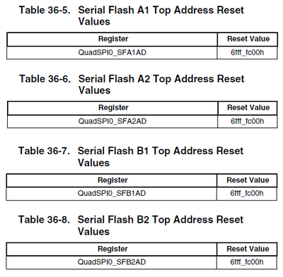
Elsewhere in the reference manual the reset values of the registers are indicated as 0x6FFFFC00:
...which seems to indicate that the top addresses are not byte counts. Instead, given that the least significant 10-bits are always 0, the most significant 22-bits are 1K block counts.
0x6FFFFC00 >> 10 is 0x1BFFFF
0x68000000 >> 10 is 0x1A0000 (The bottom address is 0x68000000)
1BFFFF - 1A0000 = 0x1FFFF (This is the 1K-block top address, and offset 128K x 1K-blocks)
The reset values place the full 128MB into Chip-A, Bank-1
Even though the QSPI peripheral itself is capable of handling 4 dies, programmers like Segger's J-Link only address 2 dies. I will therefore assume that no-one has designed their board with 4 dies.
So, assuming single- or dual-die only, and given that Segger fixes the address ranges for each bank at 64MB we can ALWAYS set the registers as follows:
QSPI_SFA1AD = 6BFFFC00 [TPDA1 = 1AFFFF] (64MB)
QSPI_SFA2AD = 6BFFFC00 [TPDA2 = 1AFFFF] (0)
QSPI_SFB1AD = 6FFFFC00 [TPDB1 = 1BFFFF] (64MB)
QSPI_SFB2AD = 6FFFFC00 [TPDB2 = 1BFFFF] (0)
This is irrespective of the die sizes. It is therefore important that memory origins and sizes in your linker scripts correctly match the ranges as per in installed chip, and not those set in the QSPI top-address registers.
/* Example for a board with a dual(2x) 64MB flash chip with 2x 1MB XiP: */
MEMORY
{
PROGRAM_FLASH   (rx) : ORIGIN = 0x00000000, LENGTH = 0x00040000 /* 256K */
EXT_PGM_FLASH_A (rx) : ORIGIN = 0x04000000, LENGTH = 0x00100000 /* 1M   */
EXT_PGM_FLASH_B (rx) : ORIGIN = 0x08000000, LENGTH = 0x00100000 /* 1M   */
SRAM_LOWER     (rwx) : ORIGIN = 0x1fff0000, LENGTH = 0x00010000 /* 64K  */
SRAM_UPPER     (rwx) : ORIGIN = 0x20000000, LENGTH = 0x00030000 /* 192K */
XIP_RESERVE_A   (rx) : ORIGIN = 0x68000000, LENGTH = 0x00100000 /* 1M   */
EXT_FILES_A     (rx) : ORIGIN = 0x68100000, LENGTH = 0x03F00000 /* 63M  */
XIP_RESERVE_B   (rx) : ORIGIN = 0x6C000000, LENGTH = 0x00100000 /* 1M   */
EXT_FILES_B     (rx) : ORIGIN = 0x6C100000, LENGTH = 0x3F0 0000 /* 63M  */
}

/* Example for a board with a dual(2x) 32MB flash chip with 2x 1MB XiP: */
MEMORY
{
PROGRAM_FLASH   (rx) : ORIGIN = 0x00000000, LENGTH = 0x00040000 /* 256K */
EXT_PGM_FLASH_A (rx) : ORIGIN = 0x04000000, LENGTH = 0x00100000 /* 1M   */
EXT_PGM_FLASH_B (rx) : ORIGIN = 0x08000000, LENGTH = 0x00100000 /* 1M   */
SRAM_LOWER     (rwx) : ORIGIN = 0x1fff0000, LENGTH = 0x00010000 /* 64K  */
SRAM_UPPER     (rwx) : ORIGIN = 0x20000000, LENGTH = 0x00030000 /* 192K */
XIP_RESERVE_A   (rx) : ORIGIN = 0x68000000, LENGTH = 0x00100000 /* 1M   */
EXT_FILES_A     (rx) : ORIGIN = 0x68100000, LENGTH = 0x01F00000 /* 31M  */
XIP_RESERVE_B   (rx) : ORIGIN = 0x6C000000, LENGTH = 0x00100000 /* 1M   */
EXT_FILES_B     (rx) : ORIGIN = 0x6C100000, LENGTH = 0x1F0 0000 /* 31M  */
}


/* Example for a board with a single 32MB flash chip with 1MB XiP: */
MEMORY
{
PROGRAM_FLASH   (rx) : ORIGIN = 0x00000000, LENGTH = 0x00040000 /* 256K */
EXT_PGM_FLASH_A (rx) : ORIGIN = 0x04000000, LENGTH = 0x00100000 /* 1M   */
SRAM_LOWER     (rwx) : ORIGIN = 0x1fff0000, LENGTH = 0x00010000 /* 64K  */
SRAM_UPPER     (rwx) : ORIGIN = 0x20000000, LENGTH = 0x00030000 /* 192K */
XIP_RESERVE_A   (rx) : ORIGIN = 0x68000000, LENGTH = 0x00100000 /* 1M   */
EXT_FILES_A     (rx) : ORIGIN = 0x68100000, LENGTH = 0x01F00000 /* 31M  */
}

