- Forums
- Product Forums
- General Purpose MicrocontrollersGeneral Purpose Microcontrollers
- i.MX Forumsi.MX Forums
- QorIQ Processing PlatformsQorIQ Processing Platforms
- Identification and SecurityIdentification and Security
- Power ManagementPower Management
- Wireless ConnectivityWireless Connectivity
- RFID / NFCRFID / NFC
- Advanced AnalogAdvanced Analog
- MCX Microcontrollers
- S32G
- S32K
- S32V
- MPC5xxx
- Other NXP Products
- S12 / MagniV Microcontrollers
- Powertrain and Electrification Analog Drivers
- Sensors
- Vybrid Processors
- Digital Signal Controllers
- 8-bit Microcontrollers
- ColdFire/68K Microcontrollers and Processors
- PowerQUICC Processors
- OSBDM and TBDML
- S32M
- S32Z/E
-
- Solution Forums
- Software Forums
- MCUXpresso Software and ToolsMCUXpresso Software and Tools
- CodeWarriorCodeWarrior
- MQX Software SolutionsMQX Software Solutions
- Model-Based Design Toolbox (MBDT)Model-Based Design Toolbox (MBDT)
- FreeMASTER
- eIQ Machine Learning Software
- Embedded Software and Tools Clinic
- S32 SDK
- S32 Design Studio
- GUI Guider
- Zephyr Project
- Voice Technology
- Application Software Packs
- Secure Provisioning SDK (SPSDK)
- Processor Expert Software
- Generative AI & LLMs
-
- Topics
- Mobile Robotics - Drones and RoversMobile Robotics - Drones and Rovers
- NXP Training ContentNXP Training Content
- University ProgramsUniversity Programs
- Rapid IoT
- NXP Designs
- SafeAssure-Community
- OSS Security & Maintenance
- Using Our Community
-
- Cloud Lab Forums
-
- Knowledge Bases
- ARM Microcontrollers
- i.MX Processors
- Identification and Security
- Model-Based Design Toolbox (MBDT)
- QorIQ Processing Platforms
- S32 Automotive Processing Platform
- Wireless Connectivity
- CodeWarrior
- MCUXpresso Suite of Software and Tools
- MQX Software Solutions
- RFID / NFC
- Advanced Analog
-
- NXP Tech Blogs
Hello all,
I am having some difficulties while searching specific information about the input capacitance of the following 56F82746VLF pins (LQFP-48):
- pin 3, configured as CLKIN0
- pin 4, configured as GPIOC1
Can anyone help me?
Thanks, Matteo
已解决! 转到解答。
Hi, Matteo,
Now I see your issue, you connect the pin3&4 together by mistake on PCB.
Generally, the pin parasitic capacitance is 1~2pF, so there is not any problem if you connect pin3&4 together.
In default, the pin4 is in GPIO input mode, it is okay. Do not configure it as GPIO output mode or XTAL mode.
Hope it can help you
BR
XiangJun Rong
Hi, Matteo,
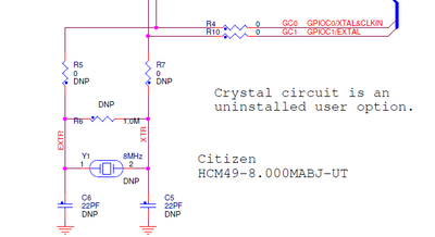
I am not clear about your question. Anyway, as you know that the MC56F82746 can connect to crystal and clock source. The crystal component is a passive, it has two pins, you can connect the crystal to the Xtal(pin4) and EXTAL(pin3) together two 22pF capacitors and one 1Mohm parallel resistor(optional) as the followng fig.
For the crystal, there is internal oscillator for the MC56F827xx so that a clock signal can be generated.
If you connect a clock source which is active device(it has independent power system can output clock signal), you can connect the clock signal to CLKIN0(pin3) directly, no capacitor is required in the case.
Hope it can help you
BR
XiangJun Rong
Hi Xiangjun,
thank you for your reply.
Actually, we are going to use a crystal oscillator with independent power supply, which goes directly on CLKIN0 as a clock source.
The specs of this oscillator say: Maximum output load capacitance = 15pF.
For technical reasons, we had to connect both pins 3 and 4 of the DSC together, so we want to be sure that the end capacitance of these pins doesn't exceed 15pF.
Can you help me?
Best regards, Matteo
Hi, Matteo,
The 15pF capacitor means that if the pin parasitic capacitances exceeds 15pF, the clock source signal will distort, it does not mean that you are required to connect an external capacitor. The less the pin capacitances is, the better the clock source signal quality is.
In conclusion, pls just connect the clock source output signal to the CLKIN0 pin(pin 3 for 48pins LQFP of LPC82746) directly, float the pin4, or use it as GPIO.
But DO NOT connect the pin3 and pin4 together.
Hope it can help you
BR
XiangJun Rong
Hi Xiangjun,
thanks for the reply, There is no additional external capacitor.
We have a batch of pcbs with pin 3 and pin 4 connected together (cannot delete connection).
Pin 3 is set as CLKIN0
Pin 4 is set as GPIOC1
My question is:
(Internal input capacitance of pin3 + Internal input capacitance of pin4) <= 15pF?
Best regards, Matteo
Hi, Matteo,
Now I see your issue, you connect the pin3&4 together by mistake on PCB.
Generally, the pin parasitic capacitance is 1~2pF, so there is not any problem if you connect pin3&4 together.
In default, the pin4 is in GPIO input mode, it is okay. Do not configure it as GPIO output mode or XTAL mode.
Hope it can help you
BR
XiangJun Rong

