- NXP Forums
- Product Forums
- General Purpose MicrocontrollersGeneral Purpose Microcontrollers
- i.MX Forumsi.MX Forums
- QorIQ Processing PlatformsQorIQ Processing Platforms
- Identification and SecurityIdentification and Security
- Power ManagementPower Management
- MCX Microcontrollers
- S32G
- S32K
- S32V
- MPC5xxx
- Other NXP Products
- Wireless Connectivity
- S12 / MagniV Microcontrollers
- Powertrain and Electrification Analog Drivers
- Sensors
- Vybrid Processors
- Digital Signal Controllers
- 8-bit Microcontrollers
- ColdFire/68K Microcontrollers and Processors
- PowerQUICC Processors
- OSBDM and TBDML
-
- Solution Forums
- Software Forums
- MCUXpresso Software and ToolsMCUXpresso Software and Tools
- CodeWarriorCodeWarrior
- MQX Software SolutionsMQX Software Solutions
- Model-Based Design Toolbox (MBDT)Model-Based Design Toolbox (MBDT)
- FreeMASTER
- eIQ Machine Learning Software
- Embedded Software and Tools Clinic
- S32 SDK
- S32 Design Studio
- Vigiles
- GUI Guider
- Zephyr Project
- Voice Technology
- Application Software Packs
- Secure Provisioning SDK (SPSDK)
- Processor Expert Software
-
- Topics
- Mobile Robotics - Drones and RoversMobile Robotics - Drones and Rovers
- NXP Training ContentNXP Training Content
- University ProgramsUniversity Programs
- Rapid IoT
- NXP Designs
- SafeAssure-Community
- OSS Security & Maintenance
- Using Our Community
-
-
Simple Calculator
- RSS フィードを購読する
- 新着としてマーク
- 既読としてマーク
- ブックマーク
- 購読
- 印刷用ページ
- 不適切なコンテンツを報告
This article presents an example of a simple application that can be created in Simulink using NXP’s Model-Based Design Toolbox (MBDT) that will be configured to run on a S32K146 board. The application will implement a calculator that can compute the sum or the product of 2 uint2_t (unsigned integer numbers represented on 2 bits).
By implementing this program, one will be able to get familiar with the toolbox NXP provides for embedded programming design. Furthermore, the implementation uses notions of finite-state machines (FSM) - for which knowledge of Stateflow is welcome -, combinatory logic, and dataflow programming.
Hardware
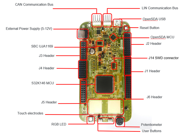
The application is built on the board S32K146 target, which comes with 2 programmable switches that the application will use as input source and an RGB LED which will be used as a form of displaying the output. The board uses the OpenSDA USB port for alimentation and for downloading the executable from the computer. No other hardware is required for programming and deploying this application.
The application can also be built on other NXP boards that come with the required programmable switches and the RGB LED.
Software
All the programming will occur on MATLAB’s Simulink which will require the following add-ons:
- MATLAB coder
- Simulink Coder
- Embedded Coder
- Embedded Coder Support Package for ARM Cortex-M Processors
- Stateflow
- NXP Model-Based Design Toolbox for S32K1xx (or the desired target)
Description
- Flow
The program gets its inputs from the 2 programmable switches presented on the board, SW2 (right user button) and SW3 (left user button). The user will introduce 1 bit at a time, by pressing the 2 switches:
- SW2 resets (0) the value of the current selection bit
- SW3 sets (1) it.
After deciding upon the value, the user will move to the next selection by pressing both switches at the same time.
The values introduced by the user are:
- the 2 operands, bit by bit, each starting with MSB (most significant bit)
- the operation – 0 for sum and 1 for product
Finally, the program will display the value of the result using the RGB LED present on the board, each color having a different meaning. In this state, moving to the next step by pressing the 2 switches will rerun the whole process of input selection.
- Display
During the bit selections the LED will show the current value of the bit:
- on (white) for 1
- off for 0
Green LED will blink between selections to announce the user that the previous bit has been successfully selected.
After the selections, the value will be represented by 5 different colors:
- yellow for 0 or 1
- red for 2 or 3
- purple for 4 or 5
- cyan for 6 or 7
- blue for 8 or 9
Design
The program is designed to work as a FSM, having the following states:
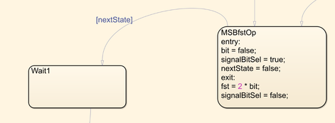
- 5 states for bit selection: MSB/LSB-fst/snd-Op and Operation
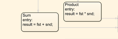
- 2 states for calculating the result: Sum/Product
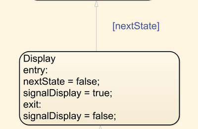
- 1 state for displaying the result: Display
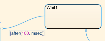
- intermediary states used to hold the green LED long enough for the user to see the transitions: Wait-x
These states can be seen in the diagram below.
Variables:
- fst - local data - stores the first operand
- snd - local data - stores the second operand
- nextState - data store memory - signal used for transitioning from the states where user input is expected (selection states and the final display state)
- bit - data store memory - the value of the bit that has been selected from the switches
- signalDisplay - data store memory - signal used to mark the final display state
- signalBitSel - data store memory - signal used to mark selection states
- result - output data - stores the result of the operation
State description:
- Operand bit selection:
- Entry: The bit is reset so that every selection begins with the value 0
- Entry: The bit selection signal is turned on to mark the selection
- Exit: The bit is assigned to its position in the number
- Exit: the selection signal is turned off
- Transition: nextState is used as a validation for transitions
- Waiting state:
- Transition: upon waiting for 100ms, the program moves to the next state
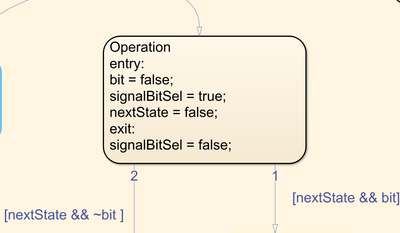
- Operation:
Similar with operand bit selection except for:
- The value of the bit is only used for transition: sum (0) or product (1)
- Operation computation:
- Display:
- Entry: signals the display state
- Exit: turns off the display signal
- Transition: based on nextState value
Input processing:
The mechanism is represented by a FSM that registers the switches pressed by the user as follows:
- If one switch press is recorded, the FSM waits a short time (25ms) for the other switch to be pressed.
- If the other switch is not pressed, then the mechanism will send the set/reset signal according to the switch recorded.
These signals are represented through a flipping value, which means that each time the value flips from 0 to 1 or 1 to 0, the program interprets the signal to be turned on.
- If the second switch is pressed, then the FSM will set the nextState variable to mark the desire of the user to move to the next state.
Note that:
- PTC12 is the name of the pin for SW2
- PTC13 is the name of the pin for SW3
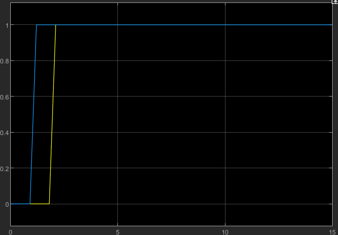
This step by step mechanism is used to compensate for the fact that the signals the 2 switches send to the processor cannot reach the value “on” at the same time no matter how much precision the user has when pressing the 2 buttons.
Notice in the figure above that when the 2 signals are unsynchronized, there is a short time where the program might only 1 signal active. In this situation, the program would interpret 2 different inputs: one where only one of the switches is pressed and 1 where both are pressed. Thus, waiting to see whether the other switch sends a signal too will solve this issue.
Bit set/reset
The set/reset functions are triggered by 2 signals:
- signalBitSel for bit selection enablement
- set/reset signal sent by the input processing mechanism
Thus these 2 signals are interpreted and put into an AND gate to check that they are active at the same time.
Notice the block between the signal and the gate (U ~= U/z) that is called “Detect change”. This block is used to detect the flip in the value of the signal. Therefore, the output of this block will be 1 only when the value flips.
Display
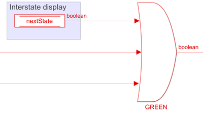
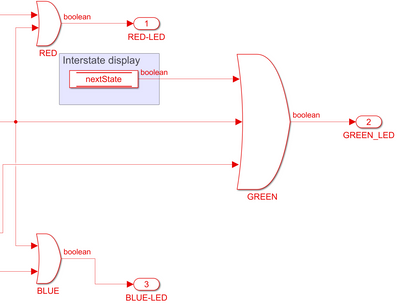
- Green LED blink
The LED will be activated by the nextState variable, which is active between 2 states in which input is to be waited from the user.
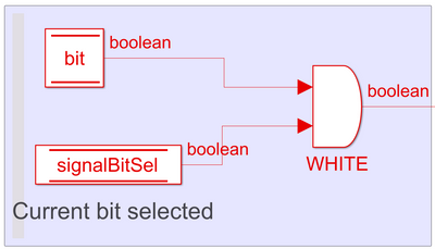
- Bit display
During the bit selection, all 3 components of the RGB LED will receive the signal of the bit (1 for on, 0 for off).
In the above circuit component, the WHITE AND gate’s output is linked to all components of the RGB LED.
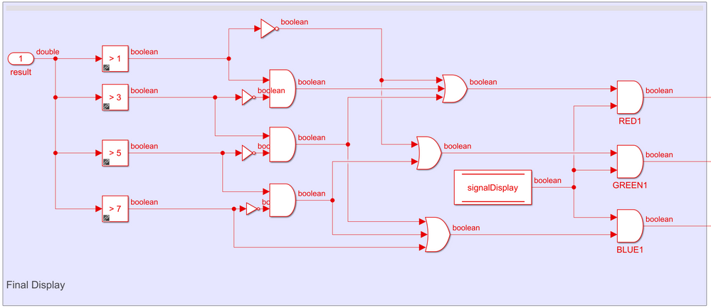
- Final display
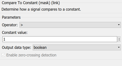
As can be seen in the block above, the result is passed through some comparison blocks to find the interval that fits it:
- result ≤ 1
- 1 < result ≤ 3
- 3 < result ≤ 5
- 5 < result ≤ 7
- 7 < result
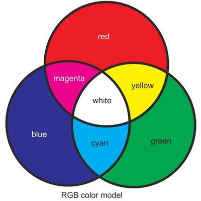
For each interval there is an AND gate that will output 1 when the result is in the correspondent interval. From there, the signal will be connected to the input of the AND gates that correspond with each color, where the “on” signal will get passed to the LED only when signalDisplay is set. The colors are formed through the following combinations:
- Yellow: red + green
- Purple: red + blue
- Cyan: green + blue
- Multiplexing the LED signals
All signals that reach the LED are being sent through an OR gate, so that each LED component will light up when one of the signals is sent.
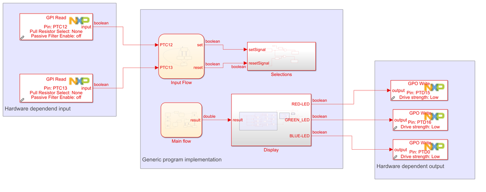
- Full view
Model
- The output (result) of the Main Flow is used by the Display block as input so that in the final Display state the correct color can be displayed on the LED.
- The signals that come from the switches are processed through the Input Flow block
- The Input Flow block will send the signals set and reset that are used by the Selections block for setting and resetting the bit.
Configuration
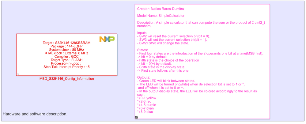
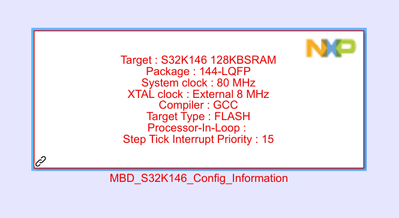
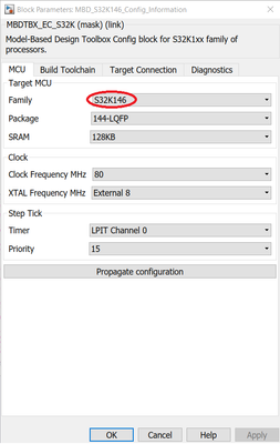
The application requires the model to have a configuration block which sets hardware configuration, the compiler and other settings for the application.
The required configurations for this application are presented in the pictures below:
Build and run
- Find Embedded Coder in the Apps tab
- In the C Code tab that will appear click on the drop-down arrow of Generate code/Build and click on build.
- For generating the C code without building the executable, click on Generate code.
If you want the executable to be downloaded on the MCU, the board must be connected to the computer via the USB port. Following the steps above will automatically download the program on the board and it will start running right after.
Demo
Check the video after the conclusion to see how the application should run on the board!
Conclusion
This application is an example of a model that can be implemented on NXP’s Model-Based Design Toolbox. The configuration is done for the application to run on a S32K146 board. This model can be extended to work with bigger numbers or with other operations, it’s up to you, sky is the limit.
I want to thank you for your interest and wish you good luck on implementing this application!
ここにコメントを追加するには、ご登録いただく必要があります。 ご登録済みの場合は、ログインしてください。 ご登録がまだの場合は、ご登録後にログインしてください。
-
101
6 -
communication standards
4 -
General Purpose Microcontrollers
19 -
i.MX RT Processors
45 -
i.MX Processors
43 -
introduction
9 -
LPC Microcontrollers
73 -
MCUXpresso
32 -
MCUXpresso Secure Provisioning Tool
1 -
MCUXpresso Conig Tools
30 -
MCUXpresso IDE
40 -
MCUXpresso SDK
25 -
Model-Based Design Toolbox
6 -
MQX Software Solutions
2 -
QorIQ Processing Platforms
1 -
QorIQ Devices
5 -
S32N Processors
4 -
S32Z|E Processors
6 -
SW | Downloads
4
- « 前へ
- 次へ »
