- NXP Forums
- Product Forums
- General Purpose MicrocontrollersGeneral Purpose Microcontrollers
- i.MX Forumsi.MX Forums
- QorIQ Processing PlatformsQorIQ Processing Platforms
- Identification and SecurityIdentification and Security
- Power ManagementPower Management
- MCX Microcontrollers
- S32G
- S32K
- S32V
- MPC5xxx
- Other NXP Products
- Wireless Connectivity
- S12 / MagniV Microcontrollers
- Powertrain and Electrification Analog Drivers
- Sensors
- Vybrid Processors
- Digital Signal Controllers
- 8-bit Microcontrollers
- ColdFire/68K Microcontrollers and Processors
- PowerQUICC Processors
- OSBDM and TBDML
-
- Solution Forums
- Software Forums
- MCUXpresso Software and ToolsMCUXpresso Software and Tools
- CodeWarriorCodeWarrior
- MQX Software SolutionsMQX Software Solutions
- Model-Based Design Toolbox (MBDT)Model-Based Design Toolbox (MBDT)
- FreeMASTER
- eIQ Machine Learning Software
- Embedded Software and Tools Clinic
- S32 SDK
- S32 Design Studio
- Vigiles
- GUI Guider
- Zephyr Project
- Voice Technology
- Application Software Packs
- Secure Provisioning SDK (SPSDK)
- Processor Expert Software
-
- Topics
- Mobile Robotics - Drones and RoversMobile Robotics - Drones and Rovers
- NXP Training ContentNXP Training Content
- University ProgramsUniversity Programs
- Rapid IoT
- NXP Designs
- SafeAssure-Community
- OSS Security & Maintenance
- Using Our Community
-
-
LPC5536 - Octal SPI, PSRAM and I3C
The LPC5536 is the newest member of the LPC55 series. I wrote an article highlighting some of the cool analog features which make the part special:
https://community.nxp.com/t5/Blogs/Introducing-the-LPC553x-It-s-all-about-the-Analog/ba-p/1438059
A singular article is simply not enough to do this component justice, so I wanted to follow up and highlight some other features that make the LPC5536 unique. I am always on the lookout for interesting microcontrollers with a special combination of peripherals. The LPC5536 family fits in the special category quite well. The analog integration, motor control subsystem, CAN-FD communications and dedicated DSP co-processor make for a powerful “industrial” processing engine. However, there are a few other important nuggets that I think are important to highlight.
Octal SPI and PSRAM with the FlexSPI Flash Controller
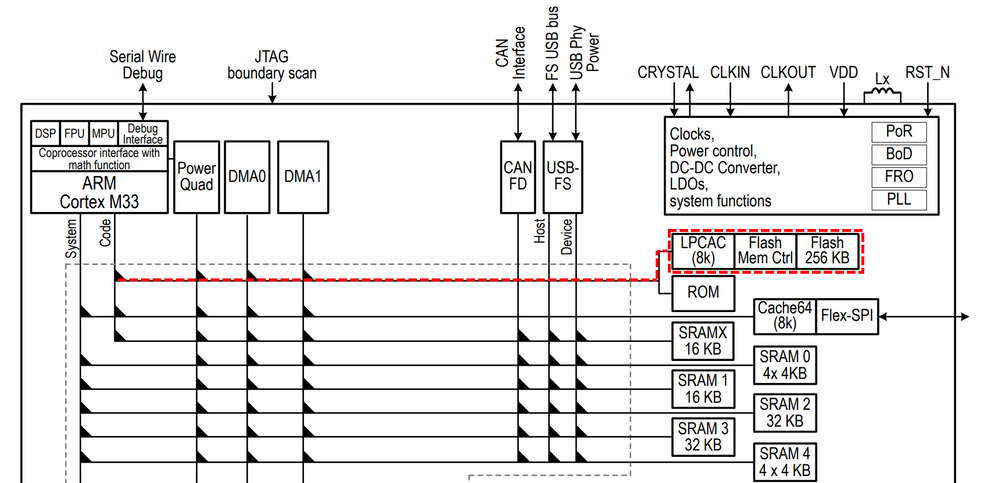
Built into the LPC5536 is 256Kb of flash memory. While the core MCU can be clocked at 150MHz, oftentimes flash memory is accessed much slower than you may initially think (up to 13 system clock flash access time for the LPC5536). The LPC5536 has an 8Kb cache/controller (LPCAC) placed in front of the flash memory array to improve performance. Performance is significantly improved with LPCAC as both instructions and data are provided to the CPU core with much lower latency.
Figure 1. LPC5536 Internal Flash Architecture.
Many applications can be well served with 256Kb of flash already built into the part. However, the total amount of memory available to the system can be expanded via the FlexSPI controller. It has been roughly 10 years ago since NXP introduced the LPC43/18 families which included a QSPI (Quad SPI) XIP(Execute-In-Place) flash controller. The XIP external flash approach has proven to be an effective way to lower the total cost of a solution while also providing large amounts of memory. An XIP flash controller handles the access to the memory device and presents itself to the system as a memory mapped device. This translation from a SPI interface to memory mapped made the LPC18/43 device families unique. With just a few extra IO lines, megabytes of flash memory could be added for code and data.
Fast forward 10 years, and the landscape of available memories is vastly larger. In addition to QSPI memories, there are now *Octal* SPI interfaces (Some under the brand name HyperFLASH™ or HyperRAM™). These memories default to a one-bit synchronous serial interface but can be configured to transfer data over an 8-bit lane. In the case of Octal SPI, data transfer can occur on *both* edges of the clock making in a DDR (Double Data Rate) memory. An Octal/Quad device which powers up in a single bit mode. A controller can then send instructions to transfer blocks of data in a synchronous, parallel fashion for greater transfer rates. QSPI memory has provided a good balance between IO requirements, package size, capacity and performance. Octal SPI takes it to another level with 8-bit DDR data transfer. The single bit mode exists so ROM based bootloaders can access the devices in a known mode to readout configuration structures that can bootstrap the part to a higher speed, parallel data access mode.
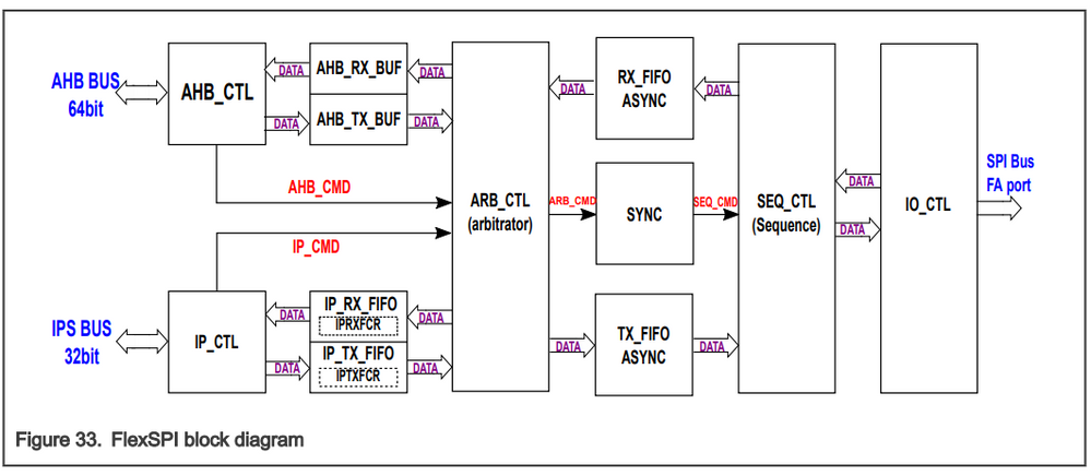
To support the wide variety of available memories in the market, NXP introduced their FlexSPI controller in the i.MX RT crossover series which is now available in the LPC5536. FlexSPI supports access to Single/Dual/Quad/Octal flash interfaces through the internal AHB bus. This means the CPU can access SPI memory as if it were a normal memory mapped flash device. The details of the SPI transactions are handled by the FlexSPI controller. FlexSPI enables a wide array of memories to be connected to the MCU and is easily adapted to new memory devices through a flexible LUT (look-up-table) based transaction system. With FlexSPI, designers have access to extremely dense flash memories and can upgrade to new flash devices as they become available. Designs can be easily scaled to storage requirements as needed. Quad/Octal SPI memories are also easy to route on a PCB as there are fewer connections. Chapter 19 of the LPC553x Reference manual details the FlexSPI controller and possible use cases.
The FlexSPI controller implementation in the LPC5536 has a single port which supports 2 physical chip select lines for up to two up to Quad SPI devices.
Figure 2. LPC5536 FlexSPI Implementation.
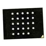
It is important to note that FlexSPI is not limited to NOR Flash memories. There are multiple vendors who offer Pseudo Static RAM (PSRAM) with Quad and Octal interfaces. PSRAM is an interesting blend of technologies. The core memory is a dynamic RAM with built in control/refresh logic. The exposed interface looks like a static RAM with Quad or Octal SPI control lines. All of the DRAM refresh details are taken care of by the internal logic. One example is an AP Memory APS6408L-OBM-BA.
Figure 3. Octal Interface PSRAM in 6mmx8mm BGA Package
This component is packaged in a small 6mm x 8mm 24 ball BGA. This footprint is common for Octal SPI memories. Note that higher speed octal devices can support up to 400MB/s transfers with a 200MHz serial clock but may require a lower voltage (+1.8v) interface. +3.3v based Quad/Octal devices are available but generally are limited to 133MHz serial clock rates. With FlexSPI, one can add quite a bit of volatile and non-volatile memory to a design without a lot of design work.
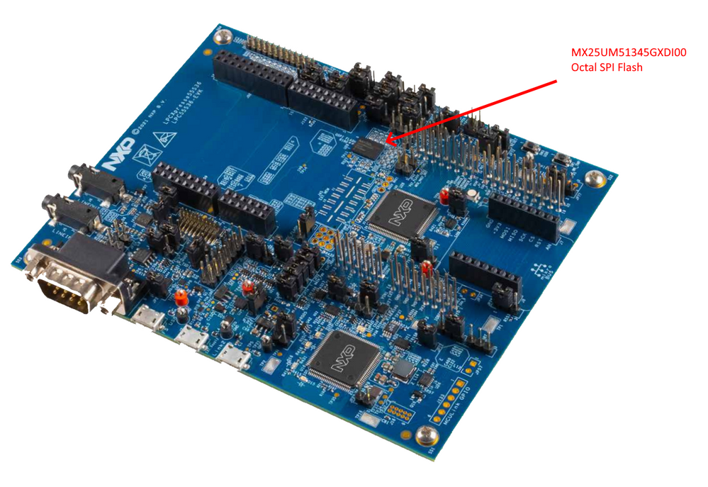
The LPC5536 EVK has a Macronix MX25UM51345GXDI00 populated to support experimentation with the FlexSPI interface.
Figure 4. LPC5536 EVK w/ MX25UM51345GXDI00 Octal SPI Flash.
The 24 Pin BGA pads supports other parts such as
- Cypress S26KS256SDPBHV02
- Cypress S27KS0641DPBHI023
- AP Memory APS6408L-OBM-BA
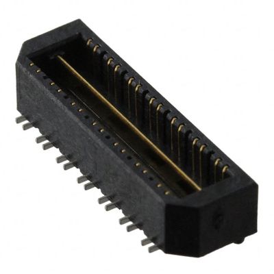
Note that the populated device runs at a lower voltage (1.9v). There are jumpers to change the IO voltage to be electrically compatible with the external flash memory. The EVK also has a dedicated expansion header to support add-on cards for users to experiment with Quad/Octal SPI devices.
Figure 5. LPC5536 EVK FlexSPI Expansion Header – Samtec QSE-014-01-F-D-DP-A
Checkout the LPC5536 EVK user manual for more details:
https://www.nxp.com/docs/en/user-guide/LPC55S36-EVKUM.pdf
FlexSPI Code Execution Speed
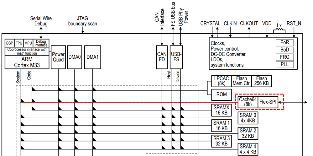
One concern that is commonly expressed with Quad/Octal SPI based design is regarding code execution speed. With the reduced number of data lines, it would initially appear that XIP operations would be slower than internal Flash. The LPC5536 FlexSPI controller includes an 8k Cache controller (CACHE64) to accelerate memory access when performing XIP. The CACHE64 block presents FlexSPI memory to the system AHB bus via a 64-bit interface.
Figure 6. LPC5536 FlexSPI Architecture w/ Cache.
NXP Application Note AN13591 provides data on XIP performance as compared to code executing from internal Flash:
https://www.nxp.com/docs/en/application-note/AN13591.pdf
Interestingly, performance is nearly identical when comparing CoreMark scores when running from Internal Flash, Octal SPI Flash or Octal SPI HyperRAM.
Figure 7. 150MHz LPC5536 w/ MX25UM51345GXDI00 Octal Flash CoreMark Score vs Internal Flash
Figure 8. 150MHz LPC5536 w/ W956D8MBYA5I Octal HyperRAM CoreMark Score vs Internal Flash.
By using CACHE64 and FlexSPI, one can achieve similar performance to internal flash memory. The distinct advantage being that once can add a significant amount of memory to the system with a small amount of PCB real estate and IO lines.
I3C - The "new" I2C
Another unique feature of the LPC5536 is the inclusion of an I3C interface (this is not a typo!). The I3C bus is a super set of the classic I2C bus. I3C was developed by the MIPI alliance to provide an upgrade to the I2C for mid-speed applications. It is positioned as an alternative to SPI while keeping a simple two wire interface between devices on a PCB. It is widely expected that I3C will be a standard interface on many new sensors and peripheral components. Some notable features:
- Up to 12MHz clock rate. SDA and SCL lines use both open-drain and push-pull modes to increase data rate and allow bi-directional communications
- “In Band Interrupts”. A peripheral can interrupt a controller over the bus without extra pins.
- Multi-Controller/Multi-Drop
- Double data rate modes that offer transfer speed on parity with classic SPI
- Hot Joins. Nodes can join the bus at any time. Nodes get notifications when a new device joins the bus.
- Backwards compatibility with I2C.
- Dynamic Addressing.
- In-Band Common Command Codes to standardize behaviors.
NXP Application Note AN13577 demonstrates a simple I3C network example:
https://www.nxp.com/docs/en/application-note/AN13577.pdf
I3C is looking very cool and offers a unique blend of I2C and SPI capabilities. Be sure to get informed on I3C as you will see a lot more of it in years to come. The additional clock speed and two-wire interface will enable some new and interesting applications. There are lots of I3C implementation details in the LPC5536 user manual so be sure to check it out.
Summary
The FlexSPI and I3C interfaces on the LPC5536 are features unique to the part as compared to other devices in the LPC55 series. The ability to add a significant amount of RAM and flash via FlexSPI allows the LPC5536 to be used in a lot of new and interesting applications. Combined with the new analog subsystem and DSP co-processor, it can be a workhorse for all your industrial and control designs. Check out the NXP website for more information about the part and the EVK:
Lastly, if you want to see code samples for the LPC5536, you can build an SDK via the MCUXpresso SDK builder:
https://mcuxpresso.nxp.com/en/welcome
You can also find LPC5536 code in the MCUXpresso Github repository:
https://github.com/NXPmicro/mcux-sdk
Cheers!
只有注册用户才能在此添加评论。 如果您已经注册,请登录。 如果您还没有注册,请注册并登录。
-
101
6 -
communication standards
4 -
General Purpose Microcontrollers
19 -
i.MX RT Processors
45 -
i.MX Processors
43 -
introduction
9 -
LPC Microcontrollers
73 -
MCUXpresso
32 -
MCUXpresso Secure Provisioning Tool
1 -
MCUXpresso Conig Tools
30 -
MCUXpresso IDE
40 -
MCUXpresso SDK
25 -
Model-Based Design Toolbox
6 -
MQX Software Solutions
2 -
QorIQ Processing Platforms
1 -
QorIQ Devices
5 -
S32N Processors
4 -
S32Z|E Processors
6 -
SW | Downloads
4
- « 前一个
- 下一个 »
