- NXP Forums
- Product Forums
- General Purpose MicrocontrollersGeneral Purpose Microcontrollers
- i.MX Forumsi.MX Forums
- QorIQ Processing PlatformsQorIQ Processing Platforms
- Identification and SecurityIdentification and Security
- Power ManagementPower Management
- MCX Microcontrollers
- S32G
- S32K
- S32V
- MPC5xxx
- Other NXP Products
- Wireless Connectivity
- S12 / MagniV Microcontrollers
- Powertrain and Electrification Analog Drivers
- Sensors
- Vybrid Processors
- Digital Signal Controllers
- 8-bit Microcontrollers
- ColdFire/68K Microcontrollers and Processors
- PowerQUICC Processors
- OSBDM and TBDML
-
- Solution Forums
- Software Forums
- MCUXpresso Software and ToolsMCUXpresso Software and Tools
- CodeWarriorCodeWarrior
- MQX Software SolutionsMQX Software Solutions
- Model-Based Design Toolbox (MBDT)Model-Based Design Toolbox (MBDT)
- FreeMASTER
- eIQ Machine Learning Software
- Embedded Software and Tools Clinic
- S32 SDK
- S32 Design Studio
- Vigiles
- GUI Guider
- Zephyr Project
- Voice Technology
- Application Software Packs
- Secure Provisioning SDK (SPSDK)
- Processor Expert Software
-
- Topics
- Mobile Robotics - Drones and RoversMobile Robotics - Drones and Rovers
- NXP Training ContentNXP Training Content
- University ProgramsUniversity Programs
- Rapid IoT
- NXP Designs
- SafeAssure-Community
- OSS Security & Maintenance
- Using Our Community
-
-
- Home
- :
- MCUXpresso Software and Tools
- :
- LPCXpresso IDE
- :
- Re: LPC54xx JTAG interface over LPC-Link2 via LPCxpresso
LPC54xx JTAG interface over LPC-Link2 via LPCxpresso
- Subscribe to RSS Feed
- Mark Topic as New
- Mark Topic as Read
- Float this Topic for Current User
- Bookmark
- Subscribe
- Mute
- Printer Friendly Page
LPC54xx JTAG interface over LPC-Link2 via LPCxpresso
- Mark as New
- Bookmark
- Subscribe
- Mute
- Subscribe to RSS Feed
- Permalink
- Report Inappropriate Content
We have designed a board based on LPC5413J256 that uses JTAG connection for debugging and program flashing. LPC5413 SWD pins are not used and are not connected to the JTAG connector. We are using LPC-Link2 to connect to the board.
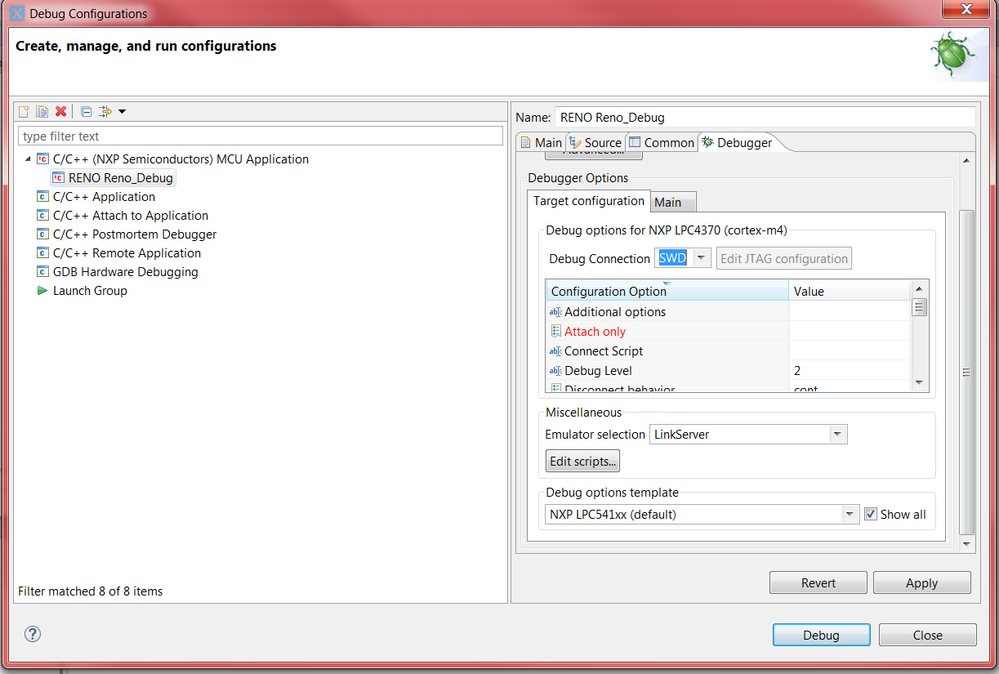
LPCxpresso has an option in "Debug options template" to select "NXP 541x (default)" which does not offer option for JTAG debugging only SWD. Since LPC5413 defaults after boot to SWD we are unable to communicate with the processor since only JTAG connection is accessible on our board.
Is there a way to switch LPC5413 programming interface from default SWD to JTAG ?
- Mark as New
- Bookmark
- Subscribe
- Mute
- Subscribe to RSS Feed
- Permalink
- Report Inappropriate Content
It looks to me like you are trying to manually create your launch configuration? If so, you don't need to - please delete.
To debug, all you should need to do is select the project in Project Explorer, then click on the Debug button in the Quickstart Panel. The IDE will then autogenerate an appropriate launch config for your part.
For more details, please read the supplied LPCXpresso IDE User Guide, or watch the videos at http://www.nxp.com/lpcxpresso.
Regards,
LPCXpresso Support
- Mark as New
- Bookmark
- Subscribe
- Mute
- Subscribe to RSS Feed
- Permalink
- Report Inappropriate Content
I am not trying to generate custom launch configuration.
For LPC54113J256 there is no option to use JTAG only SWD connection in the "Debugger" option. We have only JTAG connection wired on the board. No SWD hardware connection. We can not "talk" the uC because LPC54113J256 defaults to SWD connection.
We need to use JTAG and there is no such option for LPC54113J256 in LPCxpresso launch configuration "Debugger" tab.
- Mark as New
- Bookmark
- Subscribe
- Mute
- Subscribe to RSS Feed
- Permalink
- Report Inappropriate Content
As I said in my original reply, (according to the datasheet) there is no JTAG debugging on this part. You can only use SWD for debugging. You need to fix your circuit to bring SWD pins out...
- Mark as New
- Bookmark
- Subscribe
- Mute
- Subscribe to RSS Feed
- Permalink
- Report Inappropriate Content
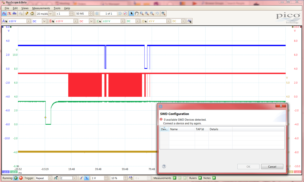
We rewired the board to communicate thru the SWD port(SDWCLK and SWDIO) plus RESET connected to the external debugger port(P1) on the NXP LPCXpresso5402 board.
All the power pins of the processor(including VDDA) are verified to be powered from 3.3V. We still are unable to communicate with LPC54113J256. Signals on the SWD bus(IO - blue, CLK - red) plus RESET(green):
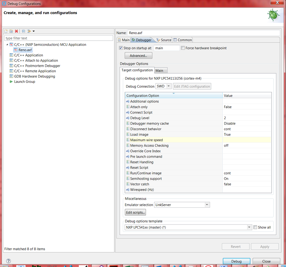
Our debug configuration:
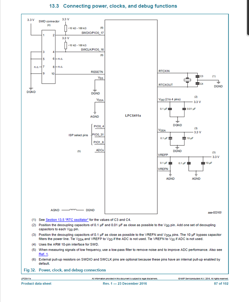
Are there any other connections needed for SWD communication outside of the ones shown in the datasheet ?:
- Mark as New
- Bookmark
- Subscribe
- Mute
- Subscribe to RSS Feed
- Permalink
- Report Inappropriate Content
Are there any requirement on ISP pins for the uC to communicate over SWD bus ? Right now our ISP0(P0_31) pin is pulled high(boot from flash).
- Mark as New
- Bookmark
- Subscribe
- Mute
- Subscribe to RSS Feed
- Permalink
- Report Inappropriate Content
Problem resolved:
1. Able to communicate over SWD(but not JTAG).
2. The problem was that code was reconfiguring SWD pins used for debugger communication. To solve the SWD communication problem, ISP0 pin was held low during reset to enter into ISP boot mode and then SWD was used to reprogram the part with code that allows SWD pins to be used in SWD mode.
- Mark as New
- Bookmark
- Subscribe
- Mute
- Subscribe to RSS Feed
- Permalink
- Report Inappropriate Content
This should help
- Mark as New
- Bookmark
- Subscribe
- Mute
- Subscribe to RSS Feed
- Permalink
- Report Inappropriate Content
We followed that document to design the board. We only missed that LPC54113J254 has JTAG for boundary scan only and needs to use SWD instead.
1. Do signals on the SWD bus look correct(in above reply) ?
2. Are there any other pins(like ISP pins) on the LPC54113J256 that need to powered/connected for SWD bus to work ? We connected the circuit to match datasheet circuit.
3. Is the external crystal oscillator enable by default on power up ?
- Mark as New
- Bookmark
- Subscribe
- Mute
- Subscribe to RSS Feed
- Permalink
- Report Inappropriate Content
According to the datasheet for LPC541xx there is no JTAG debugging support - it is SWD only. The JTAG is for boundary scan only.


