- NXP Forums
- Product Forums
- General Purpose MicrocontrollersGeneral Purpose Microcontrollers
- i.MX Forumsi.MX Forums
- QorIQ Processing PlatformsQorIQ Processing Platforms
- Identification and SecurityIdentification and Security
- Power ManagementPower Management
- MCX Microcontrollers
- S32G
- S32K
- S32V
- MPC5xxx
- Other NXP Products
- Wireless Connectivity
- S12 / MagniV Microcontrollers
- Powertrain and Electrification Analog Drivers
- Sensors
- Vybrid Processors
- Digital Signal Controllers
- 8-bit Microcontrollers
- ColdFire/68K Microcontrollers and Processors
- PowerQUICC Processors
- OSBDM and TBDML
-
- Solution Forums
- Software Forums
- MCUXpresso Software and ToolsMCUXpresso Software and Tools
- CodeWarriorCodeWarrior
- MQX Software SolutionsMQX Software Solutions
- Model-Based Design Toolbox (MBDT)Model-Based Design Toolbox (MBDT)
- FreeMASTER
- eIQ Machine Learning Software
- Embedded Software and Tools Clinic
- S32 SDK
- S32 Design Studio
- Vigiles
- GUI Guider
- Zephyr Project
- Voice Technology
- Application Software Packs
- Secure Provisioning SDK (SPSDK)
- Processor Expert Software
-
- Topics
- Mobile Robotics - Drones and RoversMobile Robotics - Drones and Rovers
- NXP Training ContentNXP Training Content
- University ProgramsUniversity Programs
- Rapid IoT
- NXP Designs
- SafeAssure-Community
- OSS Security & Maintenance
- Using Our Community
-
-
- Home
- :
- i.MX Forums
- :
- i.MX Processors
- :
- Re: How to run i.MX6/7 DDR Stress Test Tool V2.60 ?
How to run i.MX6/7 DDR Stress Test Tool V2.60 ?
- Subscribe to RSS Feed
- Mark Topic as New
- Mark Topic as Read
- Float this Topic for Current User
- Bookmark
- Subscribe
- Mute
- Printer Friendly Page
- Mark as New
- Bookmark
- Subscribe
- Mute
- Subscribe to RSS Feed
- Permalink
- Report Inappropriate Content
Dear All,
I'm trying to do stress test and RAM calibration for imx6q sbre sdb development board using i.MAX6 DDR Stress test tool V2.60 >> https://community.nxp.com/docs/DOC-105652 <<
When I go through the above link I couldn't understand how should I approach for this as I'm new to this test. So could you please provide me well detailed document for this.
**********************************************************************
>> Option 1 GUI based:
Run the GUI executable and connect your board to the host PC via USB
- Archive file: ddr_stress_tester_vX.xx.zip
- The tool will first need to run a DDR initialization script for the specified i.MX SoC (refer to Load Init Script in the GUI tool). Example initialization scripts based on NXP's development boards can be found in this zip file under the script folder. Note, these scripts may need to be modified for your custom board and memory. " <<
***********************************************************************
- What is GUI executable ?
- When I connect SABRE SDB to PC what is the port should I use ? USB OTG or Serial to USB ?
- On which hardware should I run GUI executable ? On Sabre SD or host PC ?
- Should I run DDR tester.exe on host pc or sabre sdb ?
I must be thankful to you if you will kindly reply me soon.
Regards,
Peter.
Solved! Go to Solution.
- Mark as New
- Bookmark
- Subscribe
- Mute
- Subscribe to RSS Feed
- Permalink
- Report Inappropriate Content
- Mark as New
- Bookmark
- Subscribe
- Mute
- Subscribe to RSS Feed
- Permalink
- Report Inappropriate Content
Hi All,
Dear @Oliver Chen
This is a custom hardware design with;
Processor - iMAX6Q - MCIMX6Q6AVT10AC
RAM - 933MHz Micron DDR3L - MT41K256M16TW-107 IT:P
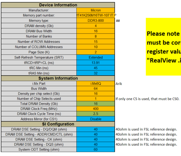
1) Here is the configuration for the script. Can you check and tell me the configurations are correct or not ?
2) Don't you have different script generator for DDR3L type memories (Low Power RAM) ?
3) In memory type I don't have to select DDR3L-933 option. What should I select ?
4) In DRAM clock frequency I don't have to select any option for 933MHz. What should I select ?
5) Under SI configuration section what should I select for
DRAM DSE Setting - DQ/DQM (ohm)
DRAM DSE Setting - ADDR/CMD/CTL (ohm)
....etc.
Can you give me an idea on this SI configuration parameters. Under which conditions of the memory should we change those values and how ?
Waiting for a detailed explanation for this.
Regards & Thanks,
Peter.
- Mark as New
- Bookmark
- Subscribe
- Mute
- Subscribe to RSS Feed
- Permalink
- Report Inappropriate Content
- Mark as New
- Bookmark
- Subscribe
- Mute
- Subscribe to RSS Feed
- Permalink
- Report Inappropriate Content
Hi Oliver Chen
We are facing the same issue in custom design board with i.MX6Quard processor and 16 bit single DDR3L ( 1Gb).
Can you please help us on it?
Thanks,
Regards,
Alpesh Mandani
- Mark as New
- Bookmark
- Subscribe
- Mute
- Subscribe to RSS Feed
- Permalink
- Report Inappropriate Content
Hi,
If you failed on calibration, it means there are some hardware unstable issues on your board. Please check your hardware.
B.R
Oliver
- Mark as New
- Bookmark
- Subscribe
- Mute
- Subscribe to RSS Feed
- Permalink
- Report Inappropriate Content
Hi Oliver,
Thanks for your quick responce.
We have followed below link guildeline for hardward design.
https://www.nxp.com/docs/en/user-guide/IMX6DQ6SDLHDG.pdf
We getting follwoung logs during DDR strees testing.
LOG:
============================================
DDR Stress Test (2.6.0)
Build: Aug 1 2017, 17:33:25
NXP Semiconductors.
============================================
============================================
Chip ID
CHIP ID = i.MX6 Dual/Quad (0x63)
Internal Revision = TO1.5
============================================
============================================
Boot Configuration
SRC_SBMR1(0x020d8004) = 0x00005878
SRC_SBMR2(0x020d801c) = 0x3a000001
============================================
ARM Clock set to 800MHz
============================================
DDR configuration
BOOT_CFG3[5-4]: 0x00, Single DDR channel.
DDR type is DDR3
Data width: 16, bank num: 8
Row size: 15, col size: 10
Chip select CSD0 is used
Density per chip select: 512MB
============================================
Current Temperature: 31
============================================
DDR Freq: 396 MHz
ddr_mr1=0x00000004
Start write leveling calibration...
running Write level HW calibration
Write leveling calibration completed, update the following registers in your initialization script
MMDC_MPWLDECTRL0 ch0 (0x021b080c) = 0x001F001F
MMDC_MPWLDECTRL1 ch0 (0x021b0810) = 0x001F001F
Write DQS delay result:
Write DQS0 delay: 31/256 CK
Write DQS1 delay: 31/256 CK
Starting DQS gating calibration
. HC_DEL=0x00000000 result[00]=0x00000011
. HC_DEL=0x00000001 result[01]=0x00000011
. HC_DEL=0x00000002 result[02]=0x00000011
. HC_DEL=0x00000003 result[03]=0x00000011
. HC_DEL=0x00000004 result[04]=0x00000011
. HC_DEL=0x00000005 result[05]=0x00000011
. HC_DEL=0x00000006 result[06]=0x00000011
. HC_DEL=0x00000007 result[07]=0x00000011
. HC_DEL=0x00000008 result[08]=0x00000011
. HC_DEL=0x00000009 result[09]=0x00000011
. HC_DEL=0x0000000A result[0A]=0x00000011
. HC_DEL=0x0000000B result[0B]=0x00000011
. HC_DEL=0x0000000C result[0C]=0x00000011
. HC_DEL=0x0000000D result[0D]=0x00000011
ERROR FOUND, we can't get suitable value !!!!
dram test fails for all values.
Error: failed during ddr calibration.
Can you please help me to resovin this issue?
Let me know if you need any more information.
Thanks,
Regards,
Alpesh Mandani
- Mark as New
- Bookmark
- Subscribe
- Mute
- Subscribe to RSS Feed
- Permalink
- Report Inappropriate Content
I am having the same issue. Please give any suggestion if anyone could find the solution to the problem. My log is as below:
Density per chip select: 1024MB
============================================
Current Temperature: 35
============================================
DDR Freq: 396 MHz
ddr_mr1=0x00000004
Start write leveling calibration...
running Write level HW calibration
Write leveling calibration completed, update the following registers in your initialization script
MMDC_MPWLDECTRL0 ch0 (0x021b080c) = 0x00150017
MMDC_MPWLDECTRL1 ch0 (0x021b0810) = 0x001F0016
MMDC_MPWLDECTRL0 ch1 (0x021b480c) = 0x00150023
MMDC_MPWLDECTRL1 ch1 (0x021b4810) = 0x00080011
Write DQS delay result:
Write DQS0 delay: 23/256 CK
Write DQS1 delay: 21/256 CK
Write DQS2 delay: 22/256 CK
Write DQS3 delay: 31/256 CK
Write DQS4 delay: 35/256 CK
Write DQS5 delay: 21/256 CK
Write DQS6 delay: 17/256 CK
Write DQS7 delay: 8/256 CK
Starting DQS gating calibration
. HC_DEL=0x00000000 result[00]=0x11011111
. HC_DEL=0x00000001 result[01]=0x11011111
. HC_DEL=0x00000002 result[02]=0x01000010
. HC_DEL=0x00000003 result[03]=0x01000010
. HC_DEL=0x00000004 result[04]=0x11111111
. HC_DEL=0x00000005 result[05]=0x11111111
. HC_DEL=0x00000006 result[06]=0x11111111
. HC_DEL=0x00000007 result[07]=0x11111111
. HC_DEL=0x00000008 result[08]=0x11111111
. HC_DEL=0x00000009 result[09]=0x11111111
. HC_DEL=0x0000000A result[0A]=0x11111111
. HC_DEL=0x0000000B result[0B]=0x11111111
. HC_DEL=0x0000000C result[0C]=0x11111111
. HC_DEL=0x0000000D result[0D]=0x11111111
ERROR FOUND, we can't get suitable value !!!!
dram test fails for all values.
Error: failed during ddr calibration
- Mark as New
- Bookmark
- Subscribe
- Mute
- Subscribe to RSS Feed
- Permalink
- Report Inappropriate Content
Dear #Oliver Chen # igorpadykov
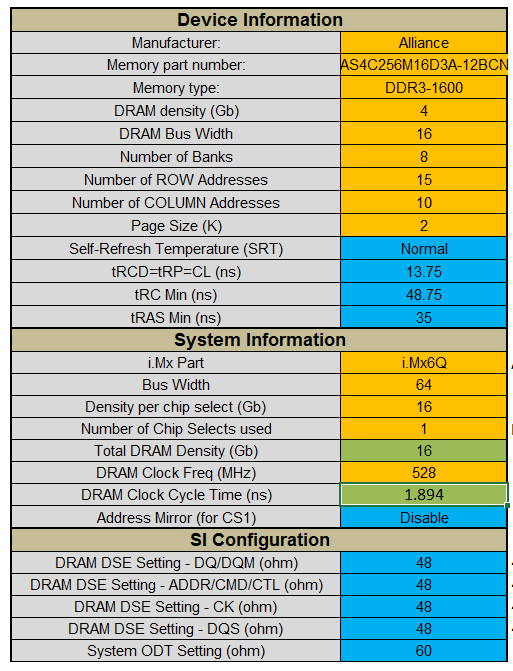
I'm using ddr_stress_tester_v2.60 software for memory calibration of Alliance AS4C256M16D3A-12BCN RAM included i.MAX6 Quad processor based custom hardware design.
This is the script changes for Alliance RAM
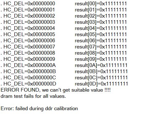
But after loading this script when I run the DDR calibration it shows following message.
What is the reason for this issue ? Is it the problem of new hard ware design ?
I must be thankful to you if you will kindly reply me as soon as possible.
Regards,
Peter.
- Mark as New
- Bookmark
- Subscribe
- Mute
- Subscribe to RSS Feed
- Permalink
- Report Inappropriate Content
Hi peteramond,
From the log, it tells us hardware board can not pass write-leveling calibration. It may be caused by bad PCB layout or incorrect DDR script setting.
From the device table, it has a 2GB DDR3 RAM with 64bit bus width and ONLY 1 chip select. It is very strange. Can you confirm it?
B.R
Oliver
- Mark as New
- Bookmark
- Subscribe
- Mute
- Subscribe to RSS Feed
- Permalink
- Report Inappropriate Content
Dear #Oliver Chen
Many thanks for your quick response.
1) Do we have any way to check the bad pcb layout ? How can we confirm this with hardware level. By measuring DRAM clock frequencies using oscilloscope?
2) Please consider the calibration run up to here >>
============================================
DDR Stress Test (2.6.0)
Build: Nov 18 2016, 23:40:32
NXP Semiconductors.
============================================
============================================
Chip ID
CHIP ID = i.MX6 Dual/Quad (0x63)
Internal Revision = TO1.2
============================================
============================================
Boot Configuration
SRC_SBMR1(0x020d8004) = 0x00000000
SRC_SBMR2(0x020d801c) = 0x21000001
============================================
ARM Clock set to 1GHz
============================================
DDR configuration
BOOT_CFG3[5-4]: 0x00, Single DDR channel.
DDR type is DDR3
Data width: 64, bank num: 8
Row size: 15, col size: 10
Chip select CSD0 is used
Density per chip select: 2048MB
============================================
Current Temperature: 51
============================================
DDR Freq: 528 MHz
ddr_mr1=0x00000000
Start write leveling calibration...
running Write level HW calibration
Write leveling calibration completed, update the following registers in your initialization script
MMDC_MPWLDECTRL0 ch0 (0x021b080c) = 0x001F001F
MMDC_MPWLDECTRL1 ch0 (0x021b0810) = 0x001F001F
MMDC_MPWLDECTRL0 ch1 (0x021b480c) = 0x001F001F
MMDC_MPWLDECTRL1 ch1 (0x021b4810) = 0x001F001F
Write DQS delay result:
Write DQS0 delay: 31/256 CK
Write DQS1 delay: 31/256 CK
Write DQS2 delay: 31/256 CK
Write DQS3 delay: 31/256 CK
Write DQS4 delay: 31/256 CK
Write DQS5 delay: 31/256 CK
Write DQS6 delay: 31/256 CK
Write DQS7 delay: 31/256 CK
Starting DQS gating calibration
. HC_DEL=0x00000000 result[00]=0x11111111
. HC_DEL=0x00000001 result[01]=0x11111111
. HC_DEL=0x00000002 result[02]=0x11111111
. HC_DEL=0x00000003 result[03]=0x11111111
. HC_DEL=0x00000004 result[04]=0x11111111
. HC_DEL=0x00000005 result[05]=0x11111111
. HC_DEL=0x00000006 result[06]=0x11111111
. HC_DEL=0x00000007 result[07]=0x11111111
. HC_DEL=0x00000008 result[08]=0x11111111
. HC_DEL=0x00000009 result[09]=0x11111111
. HC_DEL=0x0000000A result[0A]=0x11111111
. HC_DEL=0x0000000B result[0B]=0x11111111
. HC_DEL=0x0000000C result[0C]=0x11111111
. HC_DEL=0x0000000D result[0D]=0x11111111
ERROR FOUND, we can't get suitable value !!!!
dram test fails for all values.
What is the issue with this?
Error: failed during ddr calibration
3) We have used 4 RAMS and each has 4Gbit. You can get the data sheet from here >> http://www.alliancememory.com/pdf/ddr3/Alliance%20Memory_DDR3_4G_AS4C256M16D3A-12BCN_A%20die_Commerc...http://www.alliancememory.com/pdf/ddr3/Alliance%20Memory_DDR3_4G_AS4C256M16D3A-12BCN_A%20die_Commerc... <<
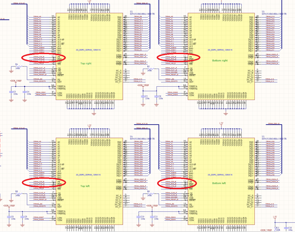
Here is the Schematic for DDR Memory part. (Please look at the red highlighted parts). Here we have used only one chip select DRAM CS0_B for every 4 RAM. That is why I have selected chip select as 1. Any mismatch with this ?
For layout design we used T topology. Please give your idea on this.
Regards & Thanks,
Peter.
- Mark as New
- Bookmark
- Subscribe
- Mute
- Subscribe to RSS Feed
- Permalink
- Report Inappropriate Content
Hi peteramond,
1) Regarding hardware layout, please follow NXP hardware design rules. If you want any documents about PCB layout guideline, please look in NXP website or contact related hardware engineers.
2) As you said, customer's board use T-topology. Do you mean star-topology? NXP recommend customer to use fly-by topology.
Alien,
Can you help to review customer's board design?
B.R
Oliver
- Mark as New
- Bookmark
- Subscribe
- Mute
- Subscribe to RSS Feed
- Permalink
- Report Inappropriate Content
Hi #Oliver Chen
"From the device table, it has a 2GB DDR3 RAM with 64bit bus width and ONLY 1 chip select. It is very strange. Can you confirm it?"
Can you comment on this ? I have used only one chip select DRAM CS0_B for every 4 RAM (For the RAM schematic in previous message). That is why I have selected chip select as 1. Any mismatch with this ?
Regards,
Peter.
- Mark as New
- Bookmark
- Subscribe
- Mute
- Subscribe to RSS Feed
- Permalink
- Report Inappropriate Content
- Mark as New
- Bookmark
- Subscribe
- Mute
- Subscribe to RSS Feed
- Permalink
- Report Inappropriate Content
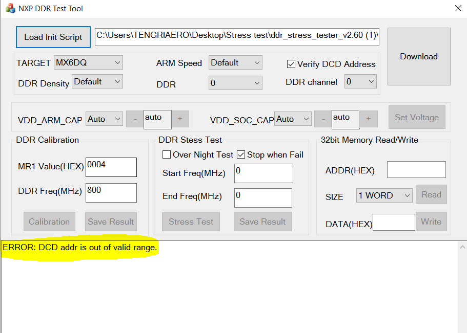
Hi peteramond,
The tool would check the address in your script is valid or invalid if 'Verify DCD Address' is selected in the GUI menu. You can remove the selection to access any address you want.
B.R
Oliver
- Mark as New
- Bookmark
- Subscribe
- Mute
- Subscribe to RSS Feed
- Permalink
- Report Inappropriate Content
Dear #Oliver Chen
Could solve the problem by commenting the following line in scrip >>
//setmem /16 0x020bc000 = 0x30
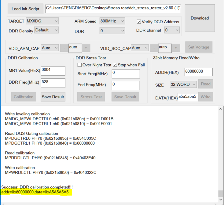
I got another issue when run the Memory Read/Write
It stuck on highlighted line.
Please advice on this.
Regards,
Peter.
- Mark as New
- Bookmark
- Subscribe
- Mute
- Subscribe to RSS Feed
- Permalink
- Report Inappropriate Content
- Mark as New
- Bookmark
- Subscribe
- Mute
- Subscribe to RSS Feed
- Permalink
- Report Inappropriate Content
Hi #Oliver Chen
Many thanks and now it is working.
- Could you please tell me how can I get full details on this ADDR, DCD address and MR1 value in DDR Calibration for each RAM. Does those things has mentioned in data sheets ?
- As well as the RAM USED IN SABRE SD >> MT41K128M16JT-125:K . And the clock frequency is 800MHz But when we put DDR Frequency as 800MHz in DDR calibration the test will fail. And the other thing is Start Frequency and end frequency. Cant we put start frequency as 750MHz and 800MHz ? It only work for up to 528MHz, Why is that ?
Regards and Thanks,
Peter.
- Mark as New
- Bookmark
- Subscribe
- Mute
- Subscribe to RSS Feed
- Permalink
- Report Inappropriate Content
Hi peteramond,
1. MR1 is the final value you used for DDR chip Mode Register MR1 when exiting from DDR write-leveling calibration operation. You can read DDR datasheet about MR1 definition. DCD address validation is just for DDR related address. If you want to write any address in script, just ignore the option. There is no problem. Don't be confused by it. DDR address range is described in i.MX6 RM memory map chapter, please read it.
2. DDR tool is an expert tool. I suggest you'd better read technical docs about DDR spec and i.MX MMDC controller chapter in RM. About your question, DDR data is triggered by both clock edge: rising edge and falling edge. When we see 800MHz noted in DDR datasheet, it means 800/2=400MHz DDR clock. For i.MX6DQ, the max DDR3 frequency is 533MHz. Don't try 750MHz/800MHz frequency, it doesn't work.
B.R
Oliver
- Mark as New
- Bookmark
- Subscribe
- Mute
- Subscribe to RSS Feed
- Permalink
- Report Inappropriate Content
Dear All,
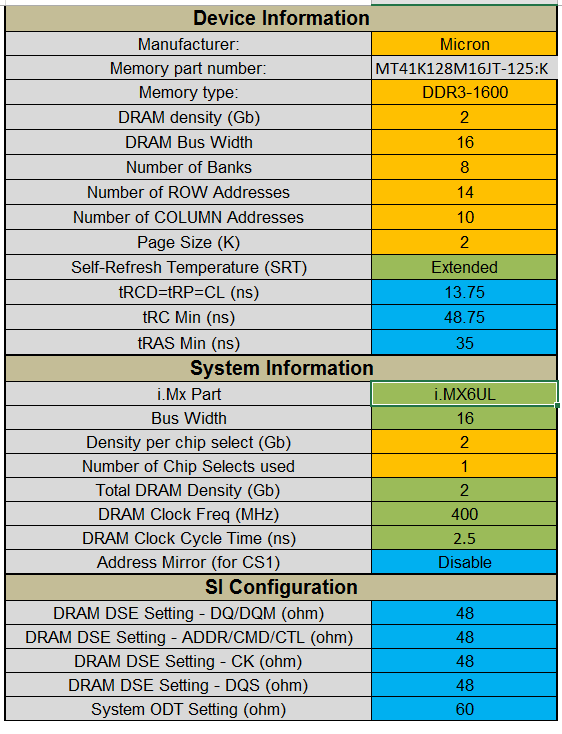
- From where can I find i.MAX6 Quad DDR3 Register Programming Aid ? Can we use the same i.MX 6UL DDR Register Programming Aid for this >> https://community.nxp.com/servlet/JiveServlet/download/329899-3-378909/I.MX6UL_DDR3_Script_Aid_V0.02... << ?
- If I'm going to use i.MAX 6UL Programming Aid I think I should change the Register Configuration table according to the RAM in Sabre SDB.
RAM USED IN SABRE SD >> MT41K128M16JT-125:K
I Edited the Register Configuration as follows >>
But NXP DDR stress tool shows following error message.
Could you please tell me the problem with this error message ? Data sheet for Micron RAM used in Sabre SD >> http://www.micron.com/~/media/documents/products/data-sheet/dram/ddr3/2gb_1_35v_ddr3l.pdf
Please advice on this.
Regards,
Peter.
- Mark as New
- Bookmark
- Subscribe
- Mute
- Subscribe to RSS Feed
- Permalink
- Report Inappropriate Content
Hi peteramond,
1. GUI executable is the PC host side software which is named DDR_Tester.exe
2. For all i.MX platform, the USB OTG port is the only necessary
3. This tool can work for all boards which USB OTG port is available.
4. DDR_Tester.exe is a PC side software.
B.R
Oliver
- Mark as New
- Bookmark
- Subscribe
- Mute
- Subscribe to RSS Feed
- Permalink
- Report Inappropriate Content
Hi igor & Oliver,
Thank you for the quick response.
I did following steps >>
But when I click "Download" it shows >>
My board is imax6 quad sabre SDB and image running on SD card is " fsl-image-validation-imx-x11-imx6qdlsolo.sdcard" . As well as I connected the sabre SDB to host pc via USB OTG of sabre sdb and then device manager shows NOTHING in user interface. As well as the loaded init script is "MX6Q_SabreSD_DDR3_1GB_64bit.inc"
Please advice on this.
Regards,
Peter.
