- NXP Forums
- Product Forums
- General Purpose MicrocontrollersGeneral Purpose Microcontrollers
- i.MX Forumsi.MX Forums
- QorIQ Processing PlatformsQorIQ Processing Platforms
- Identification and SecurityIdentification and Security
- Power ManagementPower Management
- MCX Microcontrollers
- S32G
- S32K
- S32V
- MPC5xxx
- Other NXP Products
- Wireless Connectivity
- S12 / MagniV Microcontrollers
- Powertrain and Electrification Analog Drivers
- Sensors
- Vybrid Processors
- Digital Signal Controllers
- 8-bit Microcontrollers
- ColdFire/68K Microcontrollers and Processors
- PowerQUICC Processors
- OSBDM and TBDML
-
- Solution Forums
- Software Forums
- MCUXpresso Software and ToolsMCUXpresso Software and Tools
- CodeWarriorCodeWarrior
- MQX Software SolutionsMQX Software Solutions
- Model-Based Design Toolbox (MBDT)Model-Based Design Toolbox (MBDT)
- FreeMASTER
- eIQ Machine Learning Software
- Embedded Software and Tools Clinic
- S32 SDK
- S32 Design Studio
- Vigiles
- GUI Guider
- Zephyr Project
- Voice Technology
- Application Software Packs
- Secure Provisioning SDK (SPSDK)
- Processor Expert Software
-
- Topics
- Mobile Robotics - Drones and RoversMobile Robotics - Drones and Rovers
- NXP Training ContentNXP Training Content
- University ProgramsUniversity Programs
- Rapid IoT
- NXP Designs
- SafeAssure-Community
- OSS Security & Maintenance
- Using Our Community
-
- Cloud Lab Forums
-
- Home
- :
- Product Forums
- :
- MPC5xxx
- :
- Re: How to connect the asynchronous memory of the MPC567XEVB.
How to connect the asynchronous memory of the MPC567XEVB.
- Subscribe to RSS Feed
- Mark Topic as New
- Mark Topic as Read
- Float this Topic for Current User
- Bookmark
- Subscribe
- Mute
- Printer Friendly Page
How to connect the asynchronous memory of the MPC567XEVB.
- Mark as New
- Bookmark
- Subscribe
- Mute
- Subscribe to RSS Feed
- Permalink
- Report Inappropriate Content
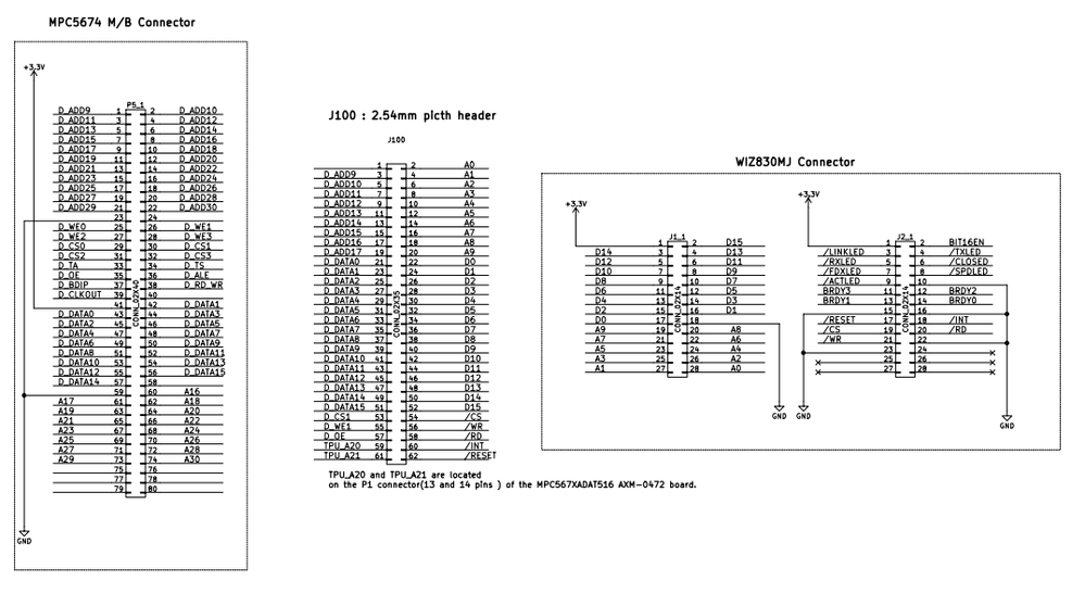
I want to control the WIZnet module with the EBI block of the MPC567XEVB.
- WIZnet modeul is WIZ830mj.
- I will connect the WIZnet module to the EBI block of the MPC5674F in the form of Asynchronous memory.
Currently, 4Mbit SRAM (CY7C1338G) is connected to EBI of MPC567XEVB.
I need some sample information related to this.
And I would like some help information if you have some example information that you can link to Asynchronous memory form EBI.
or, if you have sample imformation related to EBI, I'd like to get help.
I look forward to receiving all the help.
Thank you.
Yu-Rim Choi.
- Mark as New
- Bookmark
- Subscribe
- Mute
- Subscribe to RSS Feed
- Permalink
- Report Inappropriate Content
I could send you link on my EBI FAQs that could be helpful to you:
https://community.nxp.com/docs/DOC-101725
Looking at mentioned WIZnet module description, it is memory-like device thus it connection to EBI module should be similar.
Let me know in case specific question needs to be answered.
- Mark as New
- Bookmark
- Subscribe
- Mute
- Subscribe to RSS Feed
- Permalink
- Report Inappropriate Content
Thank you for your help first.
right , WIZnet module will be connected to EBI in the form of asynchronous memory.
As you may well know, the MPC5674XADA516 is currently connected to a 4Mbit Ram.
I will keep the 4Mbit Ram connection and want to connect the WIZnet module to EBI an asynchronous memory in the form of multiple memories.
So the detail question,
Q 1.
Reference menual(MPC5674F) has the following information.
"
29.4.1.4 Memory Controller with Support for Variou Memory Types
The EBI contains a memory controller that supports a variety of memory types, including synchronous burst mode flash and SRAM, and asynchronous/legacy flash and SRAM with compatible interface.
Eacn CS bank is configured via its own paiofor Base and Optin Register. Each time an internal to external bus cycle access is requested, the internal address is compared with the base address of each valid Base Resigister(with 17 bits having mask). See Figure 29-7. If a match is found, the attributes defind for this bank in its BR and OR are used to control t memory access. If a match is foound in more than one bank,, the lowt bank matched handles the memory access(e.g., bank 0 is selected over bank1).
"
In this part, I understood this.
Assuming that each base address is set as follow,
For example)
EBI_CAL_BR0 BA(Base Address) = 0x1000
EBI_CAL_BR1 BA(Base Address) = 0x2000
EBI_CAL_BR2 BA(Base Address) = 0x3000
EBI_CAL_BR3 BA(Base Address) = 0x4000
When reading or writing with the program as shown below, is the corresponding CS pin activated as below? (active low)
when reading or writing,
case 1. address 0x1000 = CAL_CS0 active low
case 2. address 0x2000 = CAL_CS1 active low
case 3. address 0x3000 = CAL_CS2 active low
case 4. address 0x4000 = CAL_CS3 active low
Or should I consider other correlations?
Q2 If possible can you review the circuit(data, address contol pin) I designed?
I look forward to your help.
I would really appreciate it if you could help.
Best Regards
Yu-Rim Choi.
