- NXP Forums
- Product Forums
- General Purpose MicrocontrollersGeneral Purpose Microcontrollers
- i.MX Forumsi.MX Forums
- QorIQ Processing PlatformsQorIQ Processing Platforms
- Identification and SecurityIdentification and Security
- Power ManagementPower Management
- MCX Microcontrollers
- S32G
- S32K
- S32V
- MPC5xxx
- Other NXP Products
- Wireless Connectivity
- S12 / MagniV Microcontrollers
- Powertrain and Electrification Analog Drivers
- Sensors
- Vybrid Processors
- Digital Signal Controllers
- 8-bit Microcontrollers
- ColdFire/68K Microcontrollers and Processors
- PowerQUICC Processors
- OSBDM and TBDML
-
- Solution Forums
- Software Forums
- MCUXpresso Software and ToolsMCUXpresso Software and Tools
- CodeWarriorCodeWarrior
- MQX Software SolutionsMQX Software Solutions
- Model-Based Design Toolbox (MBDT)Model-Based Design Toolbox (MBDT)
- FreeMASTER
- eIQ Machine Learning Software
- Embedded Software and Tools Clinic
- S32 SDK
- S32 Design Studio
- Vigiles
- GUI Guider
- Zephyr Project
- Voice Technology
- Application Software Packs
- Secure Provisioning SDK (SPSDK)
- Processor Expert Software
-
- Topics
- Mobile Robotics - Drones and RoversMobile Robotics - Drones and Rovers
- NXP Training ContentNXP Training Content
- University ProgramsUniversity Programs
- Rapid IoT
- NXP Designs
- SafeAssure-Community
- OSS Security & Maintenance
- Using Our Community
-
- Cloud Lab Forums
-
- Home
- :
- i.MX Forums
- :
- i.MX Processors
- :
- Re: NO SUCCESS with the OTP script - MMPF0100NPAEP
NO SUCCESS with the OTP script - MMPF0100NPAEP
- Subscribe to RSS Feed
- Mark Topic as New
- Mark Topic as Read
- Float this Topic for Current User
- Bookmark
- Subscribe
- Mute
- Printer Friendly Page
NO SUCCESS with the OTP script - MMPF0100NPAEP
- Mark as New
- Bookmark
- Subscribe
- Mute
- Subscribe to RSS Feed
- Permalink
- Report Inappropriate Content
I cannot seem to program this PMIC. PMIC part number: MMPF0100NPAEP. I am using the PF Series Programmer KITPFPGMEVME and PF0100 EVK Control GUO (Revision 3). I tried using the KITPFGUI 4.0 but it does not see any device connected.
I have successfully programmed the PMIC using the TBB script.
But have had NO SUCCESS with the OTP script.
Referring to the application note page 28 Section 3, item 3.
An 9.5 V/9.25 V, 100 mA power supply at VDDOTP bypassed by 2 x 10 μF capacitors. The voltage depends on the silicon revision used. See section OTP Programming Example for details.
What voltage should I see at VDDOTP?
My measured VDDOTP voltage measures to be 8.35 volts during programming.
I have not seen PWRON toggle ON.
My script is:
///---------------------------------------------------------------------------
// PF0100 FPGA PMIC OTP Configuration
// 6-30-2016 (Rev A)
// v1.0.0
// Set VDDOTP = 8 V, PWRON = HIGH, LICELL = 3.0 V (Optional), VIN = VDDIO = 3.3 V
//---------------------------------------------------------------------------
WRITE_I2C:7F:01 // Access PF0100 EXT Page1
//[Extended Page 1 Registers: 0xA0 - 0xAF] ----------------------------------
WRITE_I2C:A0:00 // Sw1AB Voltage = 0.300 V
WRITE_I2C:A1:14 // Sw1AB Sequence = 20
WRITE_I2C:A2:05 // Sw1AB Freq = 2 MHZ, Mode = Single phase
WRITE_I2C:A8:3F // Sw1c Voltage = 1.875 V Supplies U15
WRITE_I2C:A9:14 // Sw1c Sequence = 20
WRITE_I2C:AA:01 // Sw1c Freq = 2.0 MHZ
WRITE_I2C:AC:00 // Sw2 Voltage = 0.4 V
WRITE_I2C:AD:14 // Sw2 Sequence = 20
WRITE_I2C:AE:01 // Sw2 Freq = 2 MHZ
//[Extended Page 1 Registers: 0xB0 - 0xBF] ----------------------------------
WRITE_I2C:B0:63 // Sw3A Voltage = 2.55 V
WRITE_I2C:B1:14 // Sw3A Sequence = 20
WRITE_I2C:B2:01 // Sw3A Freq = 2 MHZ, Mode = Single phase
WRITE_I2C:B4:63 // Sw3B Voltage = 2.55 V
WRITE_I2C:B5:14 // Sw3B Sequence = 20
WRITE_I2C:B6:01 // Sw3B Freq = 2 MHZ
WRITE_I2C:B8:00 // Sw4 Voltage = 0.4 V
WRITE_I2C:B9:14 // Sw4 Sequence = 20
WRITE_I2C:BA:01 // Sw4 Freq = 2 MHZ
WRITE_I2C:BC:00 // Swbst Voltage = 5.0 V
WRITE_I2C:BD:14 // Swbst Sequence = 20
//[Extended Page 1 Registers: 0xC0 - 0xCF] ----------------------------------
WRITE_I2C:C0:00 // Vsnvs Voltage = 1.0 V
WRITE_I2C:C4:14 // Vsnvs Sequence = 20
WRITE_I2C:C8:00 // Vgen1 Voltage = 0.8 V
WRITE_I2C:C9:14 // Vgen1 Sequence = 20
WRITE_I2C:CC:00 // Vgen2 Voltage = 0.8 V
WRITE_I2C:CD:14 // Vgen2 Sequence = 20
//[Extended Page 1 Registers: 0xD0 - 0xDF] ----------------------------------
WRITE_I2C:D0:00 // Vgen3 Voltage = 1.8 V
WRITE_I2C:D1:14 // Vgen3 Sequence = 20
WRITE_I2C:D4:00 // Vgen4 Voltage = 1.8 V
WRITE_I2C:D5:14 // Vgen4 Sequence = 20
WRITE_I2C:D8:00 // Vgen5 Voltage = 1.8 V
WRITE_I2C:D9:14 // Vgen5 Sequence = 20
WRITE_I2C:DC:00 // Vgen6 Voltage = 1.8 V
WRITE_I2C:DD:14 // Vgen6 Sequence = 20
//[Extended Page 1 Registers: 0xE0 - 0xEF] ----------------------------------
WRITE_I2C:E0:07 // Power-up DVS = 6.25 mV/us, SeqCLK = 4 ms, PWRON config = 0
WRITE_I2C:E1:07 // Power-up DVS = 6.25 mV/us, SeqCLK = 4 ms, PWRON config = 0
WRITE_I2C:E2:07 // Power-up DVS = 6.25 mV/us, SeqCLK = 4 ms, PWRON config = 0
WRITE_I2C:E8:00 // Power Good = Disabled
//[Extended Page 1 Registers: 0xF0 - 0xFF] ----------------------------------
WRITE_I2C:FF:08 // I2C Device Address = 0x08
//===========================================================================
// PROGRAMMING COMMANDS FOLLOW
//===========================================================================
WRITE_I2C:E4:02 // FUSE POR=1 (This Enables OTP Programming)
WRITE_I2C:E5:02 // FUSE POR=1 (This Enables OTP Programming)
WRITE_I2C:E6:02 // FUSE POR=1 (This Enables OTP Programming)
//---------------------------------------------------------------------------
WRITE_I2C:F0:1F // Enable ECC for fuse banks 1 to 5
WRITE_I2C:F1:1F // Enable ECC for fuse banks 6 to 10
WRITE_I2C:7F:02 // Access PF0100 EXT Page2
WRITE_I2C:D0:1F // Set Auto ECC for fuse banks 1 to 5
WRITE_I2C:D1:1F // Set Auto ECC for fuse banks 6 to 10
//---------------------------------------------------------------------------
WRITE_I2C:F1:00 // Reset Bank 1 ANTIFUSE_RW and ANTIFUSE_BYPASS bits
WRITE_I2C:F2:00 // Reset Bank 2 ANTIFUSE_RW and ANTIFUSE_BYPASS bits
WRITE_I2C:F3:00 // Reset Bank 3 ANTIFUSE_RW and ANTIFUSE_BYPASS bits
WRITE_I2C:F4:00 // Reset Bank 4 ANTIFUSE_RW and ANTIFUSE_BYPASS bits
WRITE_I2C:F5:00 // Reset Bank 5 ANTIFUSE_RW and ANTIFUSE_BYPASS bits
WRITE_I2C:F6:00 // Reset Bank 6 ANTIFUSE_RW and ANTIFUSE_BYPASS bits
WRITE_I2C:F7:00 // Reset Bank 7 ANTIFUSE_RW and ANTIFUSE_BYPASS bits
WRITE_I2C:F8:00 // Reset Bank 8 ANTIFUSE_RW and ANTIFUSE_BYPASS bits
WRITE_I2C:F9:00 // Reset Bank 9 ANTIFUSE_RW and ANTIFUSE_BYPASS bits
WRITE_I2C:FA:00 // Reset Bank 10 ANTIFUSE_RW and ANTIFUSE_BYPASS bits
//---------------------------------------------------------------------------
VPGM:ON // Turn ON 9.5 V supply for PF0100A. Turn ON 9.0 V supply for PF0100.
// VPGM:ON turns on supply to the VDDOTP pin
DELAY:500 // Adds 500 msec delay to allow VPGM time to ramp up
//---------------------------------------------------------------------------
// PF0100 OTP MANUAL-PROGRAMMING (BANK 1 thru 10)
//---------------------------------------------------------------------------
// BANK 1
//---------------------------------------------------------------------------
WRITE_I2C:F1:03 // Set Bank 1 ANTIFUSE_RW and ANTIFUSE_BYPASS bits
WRITE_I2C:F1:0B // Set Bank 1 ANTIFUSE_EN
DELAY:100 // Allow 100 ms for PF0100A. Use 50 ms for PF0100.
WRITE_I2C:F1:03 // Reset Bank 1 ANTIFUSE_EN
WRITE_I2C:F1:00 // Reset Bank 1 ANTIFUSE_RW and ANTIFUSE_BYPASS bits
//---------------------------------------------------------------------------
// BANK 2
//---------------------------------------------------------------------------
WRITE_I2C:F2:03 // Set Bank 2 ANTIFUSE_RW and ANTIFUSE_BYPASS bits
WRITE_I2C:F2:0B // Set Bank 2 ANTIFUSE_EN
DELAY:100 // Allow 100 ms for PF0100A. Use 50 ms for PF0100.
WRITE_I2C:F2:03 // Reset Bank 2 ANTIFUSE_EN
WRITE_I2C:F2:00 // Reset Bank 2 ANTIFUSE_RW and ANTIFUSE_BYPASS bits
//---------------------------------------------------------------------------
// BANK 3
//---------------------------------------------------------------------------
WRITE_I2C:F3:03 // Set Bank 3 ANTIFUSE_RW and ANTIFUSE_BYPASS bits
WRITE_I2C:F3:0B // Set Bank 3 ANTIFUSE_EN
DELAY:100 // Allow 100ms for PF0100A. Use 50 ms for PF0100.
WRITE_I2C:F3:03 // Reset Bank 3 ANTIFUSE_EN
WRITE_I2C:F3:00 // Reset Bank 3 ANTIFUSE_RW and ANTIFUSE_BYPASS bits
//---------------------------------------------------------------------------
// BANK 4
//---------------------------------------------------------------------------
WRITE_I2C:F4:03 // Set Bank 4 ANTIFUSE_RW and ANTIFUSE_BYPASS bits
WRITE_I2C:F4:0B // Set Bank 4 ANTIFUSE_EN
DELAY:100 // Allow 100ms for PF0100A. Use 50 ms for PF0100.
WRITE_I2C:F4:03 // Reset Bank 4 ANTIFUSE_EN
WRITE_I2C:F4:00 // Reset Bank 4 ANTIFUSE_RW and ANTIFUSE_BYPASS bits
//---------------------------------------------------------------------------
// BANK 5
//---------------------------------------------------------------------------
WRITE_I2C:F5:03 // Set Bank 5 ANTIFUSE_RW and ANTIFUSE_BYPASS bits
WRITE_I2C:F5:0B // Set Bank 5 ANTIFUSE_EN
DELAY:100 // Allow 100 ms for PF0100A. Use 50 ms for PF0100.
WRITE_I2C:F5:03 // Reset Bank 5 ANTIFUSE_EN
WRITE_I2C:F5:00 // Reset Bank 5 ANTIFUSE_RW and ANTIFUSE_BYPASS bits
//---------------------------------------------------------------------------
// BANK 6
//---------------------------------------------------------------------------
WRITE_I2C:F6:03 // Set Bank 6 ANTIFUSE_RW and ANTIFUSE_BYPASS bits
WRITE_I2C:F6:0B // Set Bank 6 ANTIFUSE_EN
DELAY:100 // Allow 100ms for PF0100A. Use 50 ms for PF0100.
WRITE_I2C:F6:03 // Reset Bank 6 ANTIFUSE_EN
WRITE_I2C:F6:00 // Reset Bank 6 ANTIFUSE_RW and ANTIFUSE_BYPASS bits
//---------------------------------------------------------------------------
// BANK 7
//---------------------------------------------------------------------------
WRITE_I2C:F7:03 // Set Bank 7 ANTIFUSE_RW and ANTIFUSE_BYPASS bits
WRITE_I2C:F7:0B // Set Bank 7 ANTIFUSE_EN
DELAY:100 // Allow 100 ms for PF0100A. Use 50 ms for PF0100.
WRITE_I2C:F7:03 // Reset Bank 7 ANTIFUSE_EN
WRITE_I2C:F7:00 // Reset Bank 7 ANTIFUSE_RW and ANTIFUSE_BYPASS bits
//---------------------------------------------------------------------------
// BANK 8
//---------------------------------------------------------------------------
WRITE_I2C:F8:03 // Set Bank 8 ANTIFUSE_RW and ANTIFUSE_BYPASS bits
WRITE_I2C:F8:0B // Set Bank 8 ANTIFUSE_EN
DELAY:100 // Allow 100 ms for PF0100A. Use 50 ms for PF0100.
WRITE_I2C:F8:03 // Reset Bank 8 ANTIFUSE_EN
WRITE_I2C:F8:00 // Reset Bank 8 ANTIFUSE_RW and ANTIFUSE_BYPASS bits
//---------------------------------------------------------------------------
// BANK 9
//---------------------------------------------------------------------------
WRITE_I2C:F9:03 // Set Bank 9 ANTIFUSE_RW and ANTIFUSE_BYPASS bits
WRITE_I2C:F9:0B // Set Bank 9 ANTIFUSE_EN
DELAY:100 // Allow 100 ms for PF0100A. Use 50 ms for PF0100.
WRITE_I2C:F9:03 // Reset Bank 9 ANTIFUSE_EN
WRITE_I2C:F9:00 // Reset Bank 9 ANTIFUSE_RW and ANTIFUSE_BYPASS bits
//---------------------------------------------------------------------------
// BANK 10
//---------------------------------------------------------------------------
WRITE_I2C:FA:03 // Set Bank 10 ANTIFUSE_RW and ANTIFUSE_BYPASS bits
WRITE_I2C:FA:0B // Set Bank 10 ANTIFUSE_EN
DELAY:100 // Allow 100 ms for PF0100A. Use 50 ms for PF0100.
WRITE_I2C:FA:03 // Reset Bank 10 ANTIFUSE_EN
WRITE_I2C:FA:00 // Reset Bank 10 ANTIFUSE_RW and ANTIFUSE_BYPASS bits
//---------------------------------------------------------------------------
WRITE_I2C:D0:00 // Clear
WRITE_I2C:D1:00 // Clear
//---------------------------------------------------------------------------
VPGM:OFF // Turn off 8.5 V Boost Supply
DELAY:500 // Adds delay to allow VPGM to bleed off
PWRON:LOW // PWRON LOW to reload new OTP data
DELAY:500
PWRON:HIGH
//After OTP programming is complete by following the above steps, read the registers 0xA0 to 0xE8
//in Extended Page 1 and compare to the required register values as in the script. Additionally,
//read the ECC Interrupt bit, OTP_ECCI in register 0x0E. If there is an error in the programmed
//values or if the OTP_ECCI bit is set to 1, reject the part as the programming process resulted in errors.
- Mark as New
- Bookmark
- Subscribe
- Mute
- Subscribe to RSS Feed
- Permalink
- Report Inappropriate Content
Here was what being my resolve. NOT the PERFECT solution - In my case it is more of a WORKAROUND.
I believe that my target board had too much external circuitry on the 3.3V line. I did not further investigate this once I had it working. For my next board revision I will make sure to have a switch to disconnect this voltage from the external circuitry.
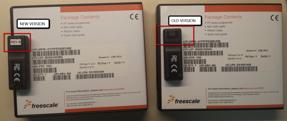
1. Using the KITPFPGMEVME REV B (Make sure that there is a sticker that says REV B)
2. I disconnected the pin on MY TARGET board that the programmer was supplying 3.3V.
3. I then Powered my TARGET board with an EXTERNAL 3.3V supply.
I verified this voltage first using a DMM. (Digital Multi Meter)
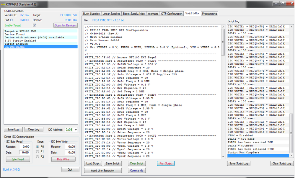
4. I opened the programming software KITPFGUI (Revision 4.2)
5. Then connected the programmer to the TARGET board and then the PC.
6. Clicked Scan for Device in the upper left corner.
7. Check the Enable Target box
8. I navigated to the Programming Tab - clicked Blank Check - Verified Device was blank
9. Navigate to the Script Editor
Load Script, Select the desired script. I posted the one used in the Original Post above.
10. Click Run Script
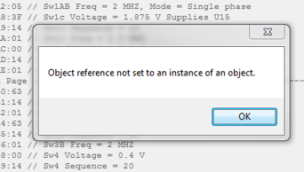
11. Uncheck Enable target when script has completed. For me a message popped up "Object reference not set to an instance of object." This was fine, my PMIC was SUCCESSFULLY programmed.
- Mark as New
- Bookmark
- Subscribe
- Mute
- Subscribe to RSS Feed
- Permalink
- Report Inappropriate Content
Hi Matthew,
The required voltage on VDDOTP is 9.5V for PF0100A like the one you are using (and 9.25V for PF0100 old versions).
Now, since the script you are using seems to be correct (you are properly sending the commands to turn on the 9.5V supply for VDDOTP, programming the banks, turning off the VPGM and toggling PWRON), I believe that the reason of why you are not able to OTP program your PMIC is because you have only 8.35V on this pin, which makes me believe that you are using a previous version of the KITPFPGMEVME programmer (this can also explain why you can only make it work with GUI version 3.0).
Unfortunately, it is not possible to program new versions of the PMIC by using an old programmer due to this reason, so, my recommendation is to check with your distributor if you can ask for a replacement for the new version of the KITPFPGMEVME programmer.
Have a great day,
Jose
-----------------------------------------------------------------------------------------------------------------------
Note: If this post answers your question, please click the Correct Answer button. Thank you!
-----------------------------------------------------------------------------------------------------------------------
- Mark as New
- Bookmark
- Subscribe
- Mute
- Subscribe to RSS Feed
- Permalink
- Report Inappropriate Content
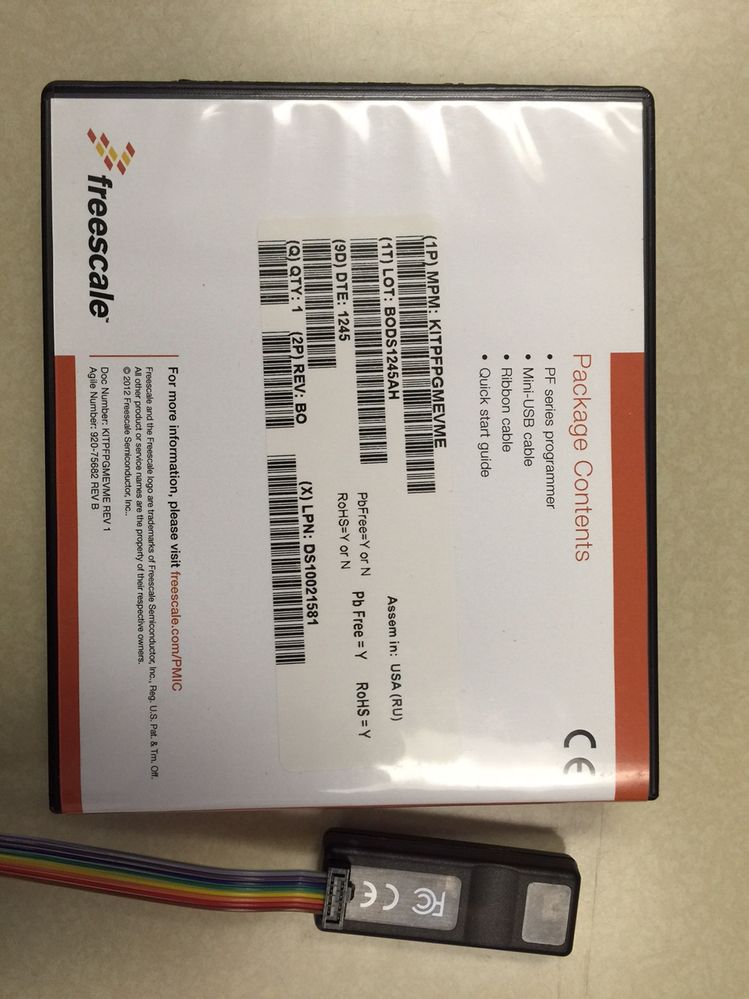
OK thanks for the replay. I will try to get a hold of a new programmer. What version is the new version? This is what I have currently:
-Matt
- Mark as New
- Bookmark
- Subscribe
- Mute
- Subscribe to RSS Feed
- Permalink
- Report Inappropriate Content
Hi Matt,
The latest revision is the KITPFPGMEVME REV B (KITPFPGMEVME should have a sticker on the bottom with “REV B” on it) like in the following image:
Have a great day,
Jose
-----------------------------------------------------------------------------------------------------------------------
Note: If this post answers your question, please click the Correct Answer button. Thank you!
-----------------------------------------------------------------------------------------------------------------------
- Mark as New
- Bookmark
- Subscribe
- Mute
- Subscribe to RSS Feed
- Permalink
- Report Inappropriate Content
Hello,
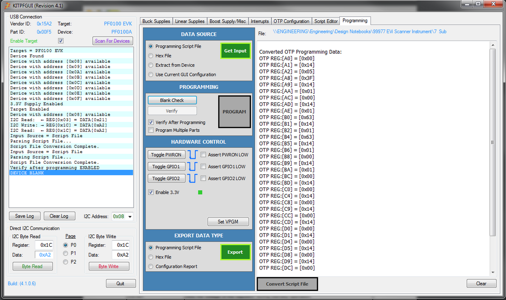
I just received my newly purchased KITPFPGMEVME REV B (Confirmed REV B Sticker). I have the 4.1 Revision of the GUI. I followed followed the procedure as described in 5.9.1 of the User Guide http://www.nxp.com/files/analog/doc/user_guide/KTPFSWUG4.pdf?fasp=1&WT_TYPE=Users%20Guides&WT_VENDOR...
I loaded the script described previously in this post and clicked the "Convert Script File" button.
The issue is the PROGRAM button never becomes available. It is GREYED out. Is there something I am missing?
I have tried using the Script Editor tab as well, by loading the script and running it in that window.
Is there something I am doing wrong?
In the image You can see that by reading REG(0x03) the data store there is 0x21 confirming the PMIC being type PF0100A . You can also see I have successfully written a value and was able to read back that value, testing the communications. I also did a Blank Check.
Thanks,
Matt
- Mark as New
- Bookmark
- Subscribe
- Mute
- Subscribe to RSS Feed
- Permalink
- Report Inappropriate Content
Hi Matt,
I think that I know what is happening in your case, are you using a KITPF0100EPEVBE + the KITPFPGMEVME? I mentioned this because the KITPFGUI is detecting it as a KITPF0100EPEVBE, this can be seen in the image you sent: “Target = PF0100 EVK” and it should be “Target = PF-Programmer”.
You can’t program the PF0100 device on the EVK. If you do, it may not function correctly (depending on what configuration you programmed in the OTP registers). For this reason the GUI developers have disabled the VPGM supply, and grayed out the [PROGRAM] button when connected to an EVK Board.
You should not be trying to connect the PF-Programmer to the EVK. The PF-Programmer works with either the Socket Board, or your own target hardware provide that have included the 8-pin header we suggest in our Users Guide.
The easiest way to verify code that they have programmed into a blank PMIC is to use the PF-Programmer, connected to a Socket Board, and navigate to the Programming tab of the GUI. Then in the DATA SOURCE select Extract from Device, and press the [Get Input] button. When the extraction is finished, navigate to the EXPORT DATA TYPE area and select Configuration Report. Press the [Export] button and fully decoded report of what they programmed will be displayed in the log screen.
Have a great day,
Jose
-----------------------------------------------------------------------------------------------------------------------
Note: If this post answers your question, please click the Correct Answer button. Thank you!
-----------------------------------------------------------------------------------------------------------------------
- Mark as New
- Bookmark
- Subscribe
- Mute
- Subscribe to RSS Feed
- Permalink
- Report Inappropriate Content
I believe that my target board had too much external circuitry on the 3.3V line. I did not further investigate this once I had it working. For my next board revision I will make sure to have a switch to disconnect this voltage from the external circuitry. If you are interested in my process to make this work: See below. One thing that still bothers me is that you stated that the program should have read the programmer as “Target = PF-Programmer”. But even once I was able to get it working it still read “Target = PF0100 EVK”. I suspect this may have to do with the OS I have on my computer. I don't know what OS for sure this programmer (KITPFPGMEVME REV B) was designed for. My system is a 64- bit Windows 7 Operating System. Thanks.
- Mark as New
- Bookmark
- Subscribe
- Mute
- Subscribe to RSS Feed
- Permalink
- Report Inappropriate Content
I am using the KITPFPGMEVME programmer (PF Series Programmer) + my own application board. The latest revision of Control GUI 4.1 does not recognize any devices (MMPF0100NPAEP) as described in Section 5.1 of the KITPFSWUG4 User guide.
I have success connecting to the device using GUI REVISION 3. Measurements taken using a DMM. (Digital Multi-meter)
| Device PIN NUM | Device PIN Name | Measured Voltage with 3.3V Supply Enabled(V) | Measured Voltage with 3.3V Supply and 8.0V Programming Supply Enabled (V) |
| 50 | VIN | 3.3 | 3.3 |
| 51 | VCOREDIG | 1.282 | 1.282 |
| 52 | VCOREREF | 1.221 | 1.221 |
| 49 | VCORE | 0 | 0 |
| 48 | GNDREF | 0 | 0 |
| 47 | VDDOTP | 0 | 8.59 |
| 55 | VDDIO | 3.3 | 3.3 |
| 54 | SCL | 3.3 | 3.3 |
| 53 | SDA | 3.3 | 3.3 |
| 56 | PWRON | 0 | 0 |
| 3 | RESETBMCU | 0 | 0 |
| 4 | STANDBY | 0.033 | 0.033 |
| 2 | SDWNB | 3.28 | 3.28 |
| 1 | INTB | 3.28 | 3.28 |
| 5 | ICTEST | 0 | 0 |


