- NXP Forums
- Product Forums
- General Purpose MicrocontrollersGeneral Purpose Microcontrollers
- i.MX Forumsi.MX Forums
- QorIQ Processing PlatformsQorIQ Processing Platforms
- Identification and SecurityIdentification and Security
- Power ManagementPower Management
- MCX Microcontrollers
- S32G
- S32K
- S32V
- MPC5xxx
- Other NXP Products
- Wireless Connectivity
- S12 / MagniV Microcontrollers
- Powertrain and Electrification Analog Drivers
- Sensors
- Vybrid Processors
- Digital Signal Controllers
- 8-bit Microcontrollers
- ColdFire/68K Microcontrollers and Processors
- PowerQUICC Processors
- OSBDM and TBDML
-
- Solution Forums
- Software Forums
- MCUXpresso Software and ToolsMCUXpresso Software and Tools
- CodeWarriorCodeWarrior
- MQX Software SolutionsMQX Software Solutions
- Model-Based Design Toolbox (MBDT)Model-Based Design Toolbox (MBDT)
- FreeMASTER
- eIQ Machine Learning Software
- Embedded Software and Tools Clinic
- S32 SDK
- S32 Design Studio
- Vigiles
- GUI Guider
- Zephyr Project
- Voice Technology
- Application Software Packs
- Secure Provisioning SDK (SPSDK)
- Processor Expert Software
-
- Topics
- Mobile Robotics - Drones and RoversMobile Robotics - Drones and Rovers
- NXP Training ContentNXP Training Content
- University ProgramsUniversity Programs
- Rapid IoT
- NXP Designs
- SafeAssure-Community
- OSS Security & Maintenance
- Using Our Community
-
-
- Home
- :
- General Purpose Microcontrollers
- :
- Kinetis Microcontrollers
- :
- Re: KL46 custom board SWD reset is never asserted
KL46 custom board SWD reset is never asserted
- Subscribe to RSS Feed
- Mark Topic as New
- Mark Topic as Read
- Float this Topic for Current User
- Bookmark
- Subscribe
- Mute
- Printer Friendly Page
- Mark as New
- Bookmark
- Subscribe
- Mute
- Subscribe to RSS Feed
- Permalink
- Report Inappropriate Content
Hi everybody,
I'm trying to program a custom board based on the KL46. However the reset signal for the SWD port is stuck at logic LOW. My programmer is a P&E Multilink FX. I can successfully program my test app on an FRDM-KL46Z. But I get the following error on CW 10.5's console when I try to program my custom KL46 board:
"can not enter background mode"
Then CW 10.5 displays the "P&E Connection Assistant" dialog offering me to "Retry", "Abort" and/or edit the connection settings. If I click "Abort" I get a "Problem Occured" dialog with the following explanation:
"Error launching imatec-firmware_FLASH_PnE U-MultiLink
ARM GDI Protocol Adapter : Can't connect. The Debugger can not connect to the P&E device"
I found a PDF guide by P&E Micro with troubleshooting steps to follow when the background mode cannot be entered:
http://cache.freescale.com/files/microcontrollers/doc/support_info/USBMLUNIVERSALFX.pdf
1) Check for power on. Checked! Power is on.
2) Make sure the processor oscillator is running. Checked! The external oscillator is not running but I believe this is normal since it should be the KL46's responsibility to cause the external crystal oscillator to run. I'm using an 8 MHz crystal.
3) Look up the startup sequence for your microprocessor:
3.a) Reset is driven low (to processor). Checked! **It always stays at low.**
3.b) Activity appears on TCK, TDI and TDO. Cheked! I'm using the SWD interface and I see that SWD_CLK and SWD_DIO give a burst sequence and then the lines go back to logic low and stay like that.
3.c) Reset is released by the interface and will go high. Checked! **Reset always stays low.**
3.d) Activity appears on TCK, TDI and TDO (Debug activity). Checked! The SWD_CLK and SWD_DIO lines stay low indefinitely.
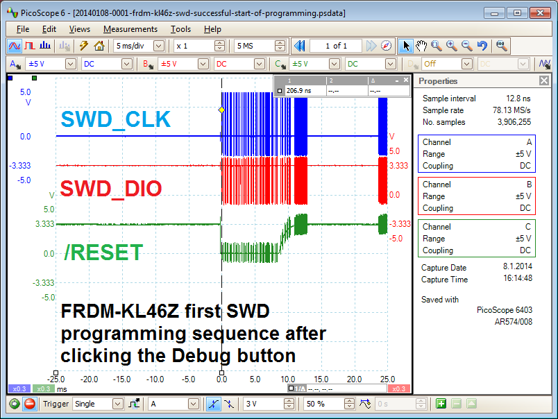
In contrast, the FRDM-KL46Z successfully passes these checks and I have been able to take oscilloscope captures of both the successful FRDM-KL46Z SWD programming attempts and the unsuccessful custom KL46 board SWD programming attempts. The burst sequence produced by the P&E Multilink FX on the SWD lines looks the same for both boards with the following exceptions:
The reset line is never asserted in the custom board and the SWD clock and data lines stay indefinitely low after the initial burst sequence.
In contrast, the burst sequence with the FRDM-KL46Z shows that the reset line is asserted at the beginning of the sequence and then it is released to logic HIGH at the end of the sequence. This is followed by an idle period and then new burst sequences are exchanged between the FRDM-KL46Z and the P&E Multilink FX.
I already checked that the SWD pins from the Multilink unit have continuity all the way the correct KL46 pins. I'm using a 64-pin LQFP package.
The pins are connected as follows:
TVCC to OUT3V3
GND to my custom board's GND plane (For example, I checked that the GND has continuity with the VSS pins on the KL46)
SWD_CLK/TCK to PTA0
SWD_DIO/TMS to PTA3
RESET_n to PTA20
TDI to PTA1
TDO to PTA2
The TDI and TDO lines are connected because that's what's shown in the FRDM-KL46Z's reference schematic. I checked these lines on an oscilloscope and I can tell that neither the FRDM-KL46Z or the custom board show any activity on them.
Thanks in advance, any suggestions are welcome! I will let you know if I find the solution.
Solved! Go to Solution.
- Mark as New
- Bookmark
- Subscribe
- Mute
- Subscribe to RSS Feed
- Permalink
- Report Inappropriate Content
Hi everybody,
The problem was fixed by fixing some solder points in the adapter board that I'm using to match the Multilink's ribbon cable to the custom board's miniature flex cable connector.
- Mark as New
- Bookmark
- Subscribe
- Mute
- Subscribe to RSS Feed
- Permalink
- Report Inappropriate Content
It makes sense since it has "carrier" on reset pin. So it may have short circuit between RESET and CLK/DIO pins.
I have same issues, but I still can not find the root cause.
- Mark as New
- Bookmark
- Subscribe
- Mute
- Subscribe to RSS Feed
- Permalink
- Report Inappropriate Content
Hello !
I'm using PE multilink universal(not FX) .
My custom KL24 board couldn't launch from multilink.
I added chip capacitors from SWDIO to GND and SWCLK to GND. ( 100pF)
I accessed target board from multilnk.
When reset pin doesn't assert , Please try to remove A 1uF capacitor of reset to GND.
So reset signal alternates H and L about 100us.
- Mark as New
- Bookmark
- Subscribe
- Mute
- Subscribe to RSS Feed
- Permalink
- Report Inappropriate Content
Hi Kenji,
Thank you for your suggestions!
Adding 100pF bypass capacitors to the SWD CLK and SWD DIO lines somehow allowed the reset line to toggle for one day but the problem is back.
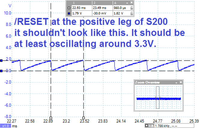
After additional tests I've come to conclude that there's something wrong with the custom board around the reset button. There's something causing the reset pin to "see" a sawtooth waveform at around 1.7 kHz, sometimes higher, sometimes lower. It depends on what I connect to the board or if I try to add larger bypass capacitors to supress this sawtooth "ripple". Also the ripple doesn't oscillate around 3.3 V. It oscillates between 0 V and 2.0 V. That's too large of an oscillation. The reset signal is probably oscillating in and out of the hysteresis zone of the KL46's reset input pin. It's ok to have some small ripple in this line but not with this kind of amplitude. So that tells me that changing my 10 kOhm pull up resistor will not completely solve this problem. In any case, I looked at an FRDM-KL46's reset and power signals and they look very clean. So I know this problem with the custom board can be cleaned up quite a bit.
Today I'm going to look further and more carefully into the custom board with an oscilloscope and a microscope to figure out the source of the problem. I will write back to let you know how the problem was solved.
- Mark as New
- Bookmark
- Subscribe
- Mute
- Subscribe to RSS Feed
- Permalink
- Report Inappropriate Content
Hi everybody,
The problem was fixed by fixing some solder points in the adapter board that I'm using to match the Multilink's ribbon cable to the custom board's miniature flex cable connector.
- Mark as New
- Bookmark
- Subscribe
- Mute
- Subscribe to RSS Feed
- Permalink
- Report Inappropriate Content
I am having a similar problem with my custom K10 board.
I, too, noticed the discrepancies in the pile of PDFs regarding the "proper" sequence to expect.
Additionally, the "square wave" on my reset line looks like yours; not square, and not 3.3V.
I was preparing to describe the signal progression, as you requested, but noticed you fixed it.
Would you mind taking a look at my layout? It is the last reply: K10 custom board
My first board was sloppy, which is probably why it didn't work.
For my revised layout, I've tried to mimic the FRDM-KL25Z as you did with the 46Z.
I'd just like to get some reassurance/confirmation on the board before I send it to fab (again).
- Mark as New
- Bookmark
- Subscribe
- Mute
- Subscribe to RSS Feed
- Permalink
- Report Inappropriate Content
- Mark as New
- Bookmark
- Subscribe
- Mute
- Subscribe to RSS Feed
- Permalink
- Report Inappropriate Content
What is the correct SWD sequence that I should see when I first click the debug button and what does this sequence mean (command by command)? Maybe this is the question I should actually be asking.
I have oscilloscope captures of a successful programming sequence for the FRDM-KL46Z board. But I don't really understand them. I have read the following documents and tutorials about SWD but I'm still not quite sure of how to apply this knowledge to analyze the SWD transfers I see for the successful programming of the FRDM-KL46Z board and the unsuccessful programming of the custom KL46 board.
Here's the documents I've read:
Serial Wire Debug and the CoreSight Debug and Trace Architecture
www.arm.com/files/pdf/Serial_Wire_Debug.pdf
NXP's Introduction to Cortex Serial Wire Debugging
http://www.lpcware.com/content/blog/introduction-cortex-serial-wire-debugging-part-one
http://www.lpcware.com/content/blog/introduction-cortex-serial-wire-debugging-part-two
http://www.lpcware.com/content/blog/introduction-cortex-serial-wire-debugging-part-three
The SWD commands I see at the beginning of the successful FRDM-KL46Z programming sequence don't seem to match the 46 cycle format mentioned in ARM's SWD document. Neither do they match the SWD unlock sequence described in NXP's SWD documentation. NXP states that these are the following steps to unlock SWD:
1) The Host needs to switch the target from JTAG to SWD mode by clocking 0xE79E onto SWDCLK/SWDIO
2) SWD connection sequence- clock out more than 50 binary 1s
3) Must read the Debug Port IDCODE register (address 0)
4) Turn on Debug Port by settings bits 28 and 30 at DP address 4
5) Write AP select (debug port address 8) to 0xF0 (to prep for AP read of 0xFC)
6) Unlock Access Port by reading AP ID register (AP address 0xFC)
If the FRDM-KL46Z's successful SWD programming sequence does not match the SWD documentation then how is it possible for the Multilink programmer to successfully program the board? Is it the case that Freescale and P&E Micro have implemented a custom or proprietary initialization sequence?
Here's the first burst sequence I see when I try to program the FRDM-K46Z board:
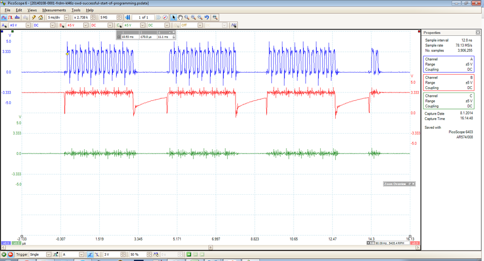
Zooming in into the first burst:
Zooming in even more on the section right after the reset is asserted:
Thanks in advance. I will keep posting any hints and discoveries in the meantime.


