- NXP Forums
- Product Forums
- General Purpose MicrocontrollersGeneral Purpose Microcontrollers
- i.MX Forumsi.MX Forums
- QorIQ Processing PlatformsQorIQ Processing Platforms
- Identification and SecurityIdentification and Security
- Power ManagementPower Management
- MCX Microcontrollers
- S32G
- S32K
- S32V
- MPC5xxx
- Other NXP Products
- Wireless Connectivity
- S12 / MagniV Microcontrollers
- Powertrain and Electrification Analog Drivers
- Sensors
- Vybrid Processors
- Digital Signal Controllers
- 8-bit Microcontrollers
- ColdFire/68K Microcontrollers and Processors
- PowerQUICC Processors
- OSBDM and TBDML
-
- Solution Forums
- Software Forums
- MCUXpresso Software and ToolsMCUXpresso Software and Tools
- CodeWarriorCodeWarrior
- MQX Software SolutionsMQX Software Solutions
- Model-Based Design Toolbox (MBDT)Model-Based Design Toolbox (MBDT)
- FreeMASTER
- eIQ Machine Learning Software
- Embedded Software and Tools Clinic
- S32 SDK
- S32 Design Studio
- Vigiles
- GUI Guider
- Zephyr Project
- Voice Technology
- Application Software Packs
- Secure Provisioning SDK (SPSDK)
- Processor Expert Software
-
- Topics
- Mobile Robotics - Drones and RoversMobile Robotics - Drones and Rovers
- NXP Training ContentNXP Training Content
- University ProgramsUniversity Programs
- Rapid IoT
- NXP Designs
- SafeAssure-Community
- OSS Security & Maintenance
- Using Our Community
-
-
- Home
- :
- General Purpose Microcontrollers
- :
- LPC Microcontrollers
- :
- Re: SDRAM and NOR Flash Sample / Reference code for Understanding the functionality
SDRAM Reference code for Understanding the functionality
- Subscribe to RSS Feed
- Mark Topic as New
- Mark Topic as Read
- Float this Topic for Current User
- Bookmark
- Subscribe
- Mute
- Printer Friendly Page
SDRAM Reference code for Understanding the functionality
- Mark as New
- Bookmark
- Subscribe
- Mute
- Subscribe to RSS Feed
- Permalink
- Report Inappropriate Content
Hi Jeremy,
I am using LPC4367 controller with MCU Xpresso 10.3.0_2200. I am using SDRAM and NOR Flash interface in one of our projects. I was working with Evaluation board OM13088 but it that board no SDRAM and NOR flash interface is avialable. I am using SDRAM and NOR flash both interfaced with EMC lines aviable in LPC4367 controller.
I refered the code in e lpcopen_3_02_lpcxpresso_mcb4357 and also refered periph_memtest and misc_spifi_tst demos. But there is no EMC init routine avialable. Is there any sample code or a reference code for SDRAM with proper intitiatilization routine.
Also i want to allocate one of my Buffer to SDRAM address, i got the information related to it i MCU expresso User guied but still i want to know than as we user
__At(Address) attribute in Keil to allocate the array or a buffer like
uint16_t Buffer[1024] __at(0x28000000)
In the similar manner how we can use it in MCU Expresso . I have downloaded MCUxpresso 10.3.0 .
To conclude i want the sample or areference code for SDRAM and NOR flash with proper EMC init routine which not provided in existing reference code
I need this since i want to test my development board which is ready. So please consider it on higher priority. Mean while i am trying to refere other forums as well for my understanding.
Thanks
Gaurav More
- Mark as New
- Bookmark
- Subscribe
- Mute
- Subscribe to RSS Feed
- Permalink
- Report Inappropriate Content
Hi Gaurav More,
Thanks for your reply.
32-bit aligned is inspired by the periph_memtest demo, in the demo, it illustrates the similar testing as you did.
Actually, I don't find the video you attach, please check it.
Have a great day,
TIC
-------------------------------------------------------------------------------
Note:
- If this post answers your question, please click the "Mark Correct" button. Thank you!
- We are following threads for 7 weeks after the last post, later replies are ignored
Please open a new thread and refer to the closed one, if you have a related question at a later point in time.
-------------------------------------------------------------------------------
- Mark as New
- Bookmark
- Subscribe
- Mute
- Subscribe to RSS Feed
- Permalink
- Report Inappropriate Content
- Mark as New
- Bookmark
- Subscribe
- Mute
- Subscribe to RSS Feed
- Permalink
- Report Inappropriate Content
Hi Gaurav More,
Sorry for reply late.
Actually, I also have no idea about this weird phenomenon.
Does the code work well in non-debug mode?
If you have a logic analyzer on hand, I'd highly recommend you to visualize the SDRAM's operation via the logic analyzer, it may give you an insight into this phenomenon.
Have a great day,
TIC
-------------------------------------------------------------------------------
Note:
- If this post answers your question, please click the "Mark Correct" button. Thank you!
- We are following threads for 7 weeks after the last post, later replies are ignored
Please open a new thread and refer to the closed one, if you have a related question at a later point in time.
-------------------------------------------------------------------------------
- Mark as New
- Bookmark
- Subscribe
- Mute
- Subscribe to RSS Feed
- Permalink
- Report Inappropriate Content
Hi Jeremy,
I did following exercise with SDRAM,
1. I write 0xA5A5 and 0x1234 alternately from Address 0x28000000 for 0 to 127 location and checked, then it writes properly.
2. Then I did the same exercise byt changing the address to 0x28000100 for 0 to 127 location and checked, then it writes properly.
But when after writing from 0x28000100 location i check whether the data written from 0x28000000 is there or not. then I found the that data was corrupted. so over all 2 observations
1. Able to write only 256 bytes but when trying to write fro next 256 address it is writng only 256 bytes but also corrupting the previous address data.
Is there any possibility to check the same SDRAM on MCB4357 board by replaceing the exixting SDRAM on the Evaluation board at your side? this will confirm that the is problem with the code and not with the lines. i have attached the PDF of the SDRAM I am using as interface.
I need to conclude whether to go ahead with this controller or not since all other peripherals are workign except NOR flash an SDRAM which are used in EMC mode. I check with QSPI flash it is working with the library code provide by LPC Xpresso. If similar code and interface avilable for the SDRAM then it will be help ful. Looking at the evaluation board it seem possible to replace SDRAM.
I have already given my customized board to nxp to Nikhil Ullal at bangalore. You can co-ordiante with him regarding the behaviour i ahve shared.
Thanks
Gaurav More
- Mark as New
- Bookmark
- Subscribe
- Mute
- Subscribe to RSS Feed
- Permalink
- Report Inappropriate Content
Hi Gaurav More
Thanks for your reply.
Q1) Do we have a sample code for NOR flash interface with any other controller apart from LPC4367?
-- In the periph_memtest demo, it's also initialized the parallel flash, it's available to be testing as doing for the SDRAM. In addition, I've attached a demo which describes how to use EMC to program the external Nor Flash, note that: the demo is base on Keil and IAR.
Have a great day,
TIC
-------------------------------------------------------------------------------
Note:
- If this post answers your question, please click the "Mark Correct" button. Thank you!
- We are following threads for 7 weeks after the last post, later replies are ignored
Please open a new thread and refer to the closed one, if you have a related question at a later point in time.
-------------------------------------------------------------------------------
- Mark as New
- Bookmark
- Subscribe
- Mute
- Subscribe to RSS Feed
- Permalink
- Report Inappropriate Content
Hi Jeremy,
Thanks for the reply and the code you sent for the reference. I am refering the code and making modifcations as per the demo code.
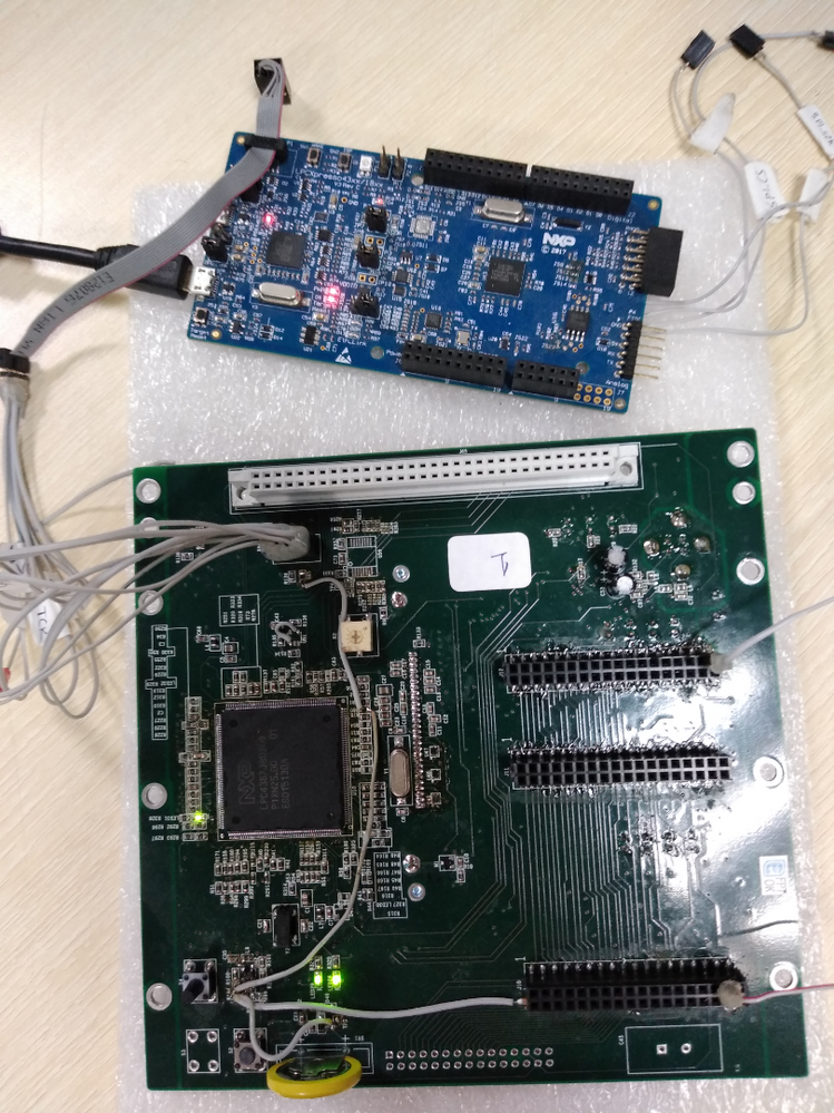
But the SDRAM code debug behaviour is still open. I am attaching the setup for debuging where you can see that I am using OM13088 Evaluation board for debugging by development board.
Here you can see that the evalboard OM13088 for LPC4367 is used to debug the development board. Also i am attaching the vedio of the behaviour while debugging the code.
The details of the vedio is as follows, whic you can see it in the vedio but feww thing i want to highlight while watching the vedio,
1. When I uploaded the code for debugging and run the code without any break point. at that time the code is working fine. You can see the LED toggling as per the code logic.
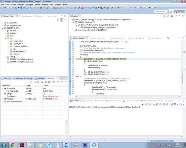
2. Now when I stop the code then it stoped at for loop, there you can see the at the data_buffer I want to store 0x0B and that too in only 20 arrays but the expression shows that it has stored in all the array location which is not expected as per the logic.
#define DRAM_SIZE 20
Length = DRAM_SIZE;
for (i=0;i<Length; i++)
{
data_buffer[i] = 0x0B;
}
This is the first issue.
3. The second issue, When I put the break to other locationa after stopping the code to check the value then you can see the behaviour, It is not tracable . it shows some error which is not understanding.
4. And the last one is when i stop the code again to trace the program counter then the code gets terminated.
but again when I run the code after removing teh debugger then it runs well as per the code logic.
I am attaching both the vedios
1. Debug behaviour (SDRAM_debugvedio.zip)
2. After reset the board by removing the debugger,
This is critical since i need to integrate the module in my project but if the debug behaviour is like this then it is deficult for the to proceed. Also refer the attached code w.r.t the settings required for debugging.
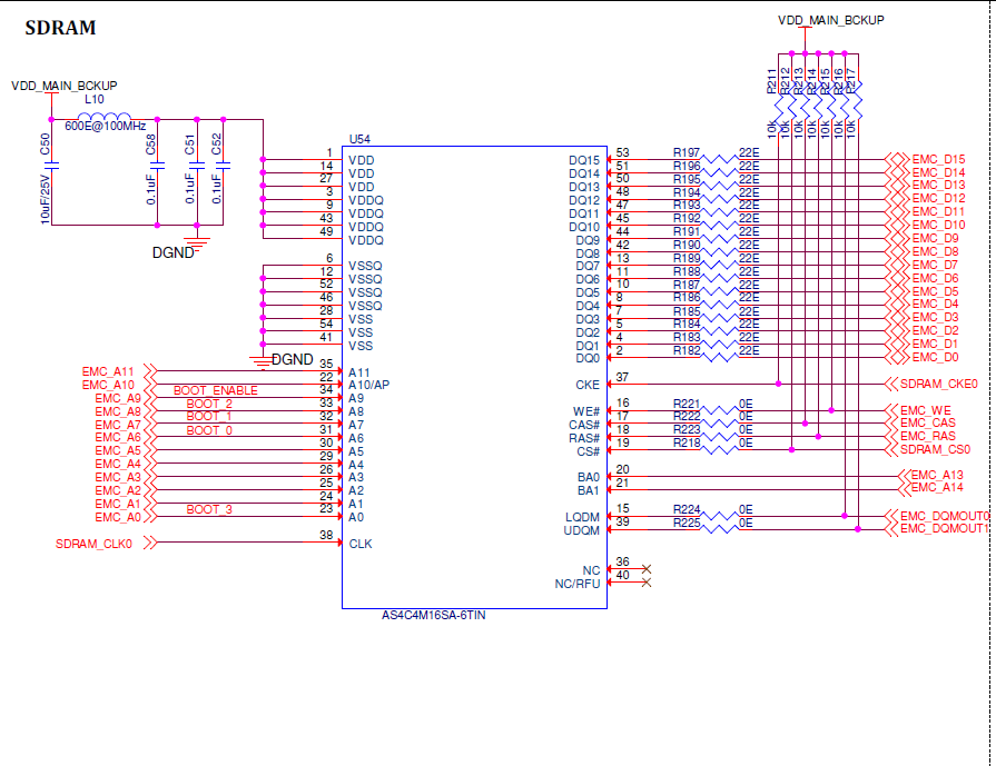
I am using SDRAM (AS4C4M16SA-6TIN ) for your reference. Also let me know if I am missing any settings. Mean while I will work with the NOR flash code as per the demo code.
Thanks
Gaurav More
- Mark as New
- Bookmark
- Subscribe
- Mute
- Subscribe to RSS Feed
- Permalink
- Report Inappropriate Content
Hi Gaurav More
Thanks for your reply.
According to your reply, the demo will work well while debugging, however, it may encounter some weird phenomenon when placing some breakpoints, is that right?
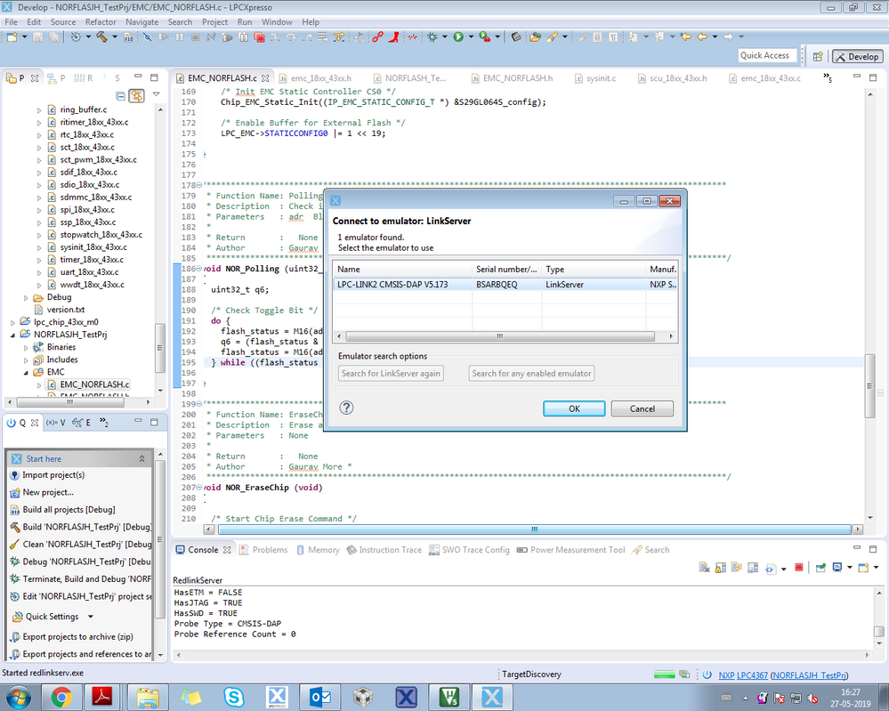
What's the firmware the LPC4367 run with, CMSIS-DAP or Jlink?
Have a great day,
TIC
-------------------------------------------------------------------------------
Note:
- If this post answers your question, please click the "Mark Correct" button. Thank you!
- We are following threads for 7 weeks after the last post, later replies are ignored
Please open a new thread and refer to the closed one, if you have a related question at a later point in time.
-------------------------------------------------------------------------------
- Mark as New
- Bookmark
- Subscribe
- Mute
- Subscribe to RSS Feed
- Permalink
- Report Inappropriate Content
Hi Jeremy,
1) It worked well when it is free running. which you already seen and when I put a breakpoint in between to check the values then it is behaving some what different. Also it is just a demo code and no other modules are running in parallel with that.
Especially for me this is one concern regarding the fill part
I want to store 0x0B and that too in only 20 arrays but the expression shows that it has stored in all the array location which is not expected as per the logic.
#define DRAM_SIZE 20
Length = DRAM_SIZE;
for (i=0;i<Length; i++)
{
data_buffer[i] = 0x0B;
}
2) What's the firmware the LPC4367 run with, CMSIS-DAP or Jlink?
Also you can comment on the setup but for me i am able to debug but then it there any dependency of the debugger?
also have check the project is there any such issue whic can trigger the kind of behaviour?
Thanks
Gaurav More
- Mark as New
- Bookmark
- Subscribe
- Mute
- Subscribe to RSS Feed
- Permalink
- Report Inappropriate Content
Hi Gaurav More,
Thank you for your interest in NXP Semiconductor products and for the opportunity to serve you.
I've answered the question in the thread (SDRAM and NOR Flash Sample / Reference code for Understanding the functionality ), please check it.
Have a great day,
TIC
-----------------------------------------------------------------------------------------------------------------------
Note: If this post answers your question, please click the Correct Answer button. Thank you!
-----------------------------------------------------------------------------------------------------------------------
- Mark as New
- Bookmark
- Subscribe
- Mute
- Subscribe to RSS Feed
- Permalink
- Report Inappropriate Content
Hi Jeremy,
Any inputs regarding the query. It is required for the project development. Need to any modifications required since some times it runs a complete while and agian while repeating the same statement it crashes,
while(1)
{
StardAddr = (uint32_t *)EMC_ADDRESS_DYCS0;
for(i=0; i<20; i++)
{
*StardAddr = 0x55AA55AA;
StardAddr++;
}
for (i=0; i<0xFFFF;i++ );
for (i=0; i<0xFFF;i++ );
#if 1
StardAddr1 = (uint32_t *)EMC_ADDRESS_DYCS0;
for(i=0; i<Length; i++)
{
ReadData[i] = (uint32_t)*StardAddr1;
if(ReadData[i] != *StardAddr1)
{
while(1)
{
Chip_GPIO_SetPinToggle(LPC_GPIO_PORT, 5, 19);
for (i=0; i<0xFFFFF;i++ );
}
}
StardAddr1++;
}
#endif
refer the code attached inthe above post.
Thanks
Gaurav More
- Mark as New
- Bookmark
- Subscribe
- Mute
- Subscribe to RSS Feed
- Permalink
- Report Inappropriate Content
Hi Gaurav More,
Thanks for your reply.
I'd like to know which board you run the code for testing, in further,
whether you can replicate the crash event every time.
Have a great day,
TIC
-------------------------------------------------------------------------------
Note:
- If this post answers your question, please click the "Mark Correct" button. Thank you!
- We are following threads for 7 weeks after the last post, later replies are ignored
Please open a new thread and refer to the closed one, if you have a related question at a later point in time.
-------------------------------------------------------------------------------
- Mark as New
- Bookmark
- Subscribe
- Mute
- Subscribe to RSS Feed
- Permalink
- Report Inappropriate Content
Hi Jeremy,
I am working on my customized board. I refered AN11508 for SDRAM modification and I am using AS4C4M16SA-C&I , 64M – (4M x 16 bit) Synchronous DRAM (SDRAM)
I also refered follwing links,
https://community.nxp.com/thread/435767
https://community.nxp.com/thread/418570
https://community.nxp.com/thread/420158
https://community.nxp.com/thread/420806
Based on these links I made modifications in my code. Also find the schematics for development board based on the AN11508.pdf
Also now I made slight modification with respect to the EMC_CLK0. I changed for EMC_CLK0 to EMC_CLK1. Rest all the connections are same.
Now after doing this modification I am facing problem with respect to the code execution. I am writing data to the SDRAM location using the following method,
#define DRAM_SIZE 20//(8 * 1024 * 1024)
#define EMC_ADDRESS_DYCS0 (0x28000000)
uint16_t *StardAddr,
uint16_t Length = DRAM_SIZE;
uint16_t ReadData[DRAM_SIZE];
uint16_t WriteData[DRAM_SIZE];
unsigned long i = 0;
while(1)
{
StardAddr = (uint16_t *)EMC_ADDRESS_DYCS0;
for(i=0; i<20; i++)
{
*StardAddr = 0x55AA;
StardAddr++;
}
for (i=0; i<0xFFFF;i++ );
for (i=0; i<0xFFF;i++ );
StardAddr = (uint16_t *)EMC_ADDRESS_DYCS0;
for(i=0; i<Length; i++)
{
ReadData[i] = *StardAddr1;
if(ReadData[i] != *StardAddr)
{
while(1)
{
Chip_GPIO_SetPinToggle(LPC_GPIO_PORT, 5, 19);
for (i=0; i<0xFFFFF;i++ );
}
}
StardAddr++;
}
}/* EOF While*/
Here is the process and the observations while running the code.
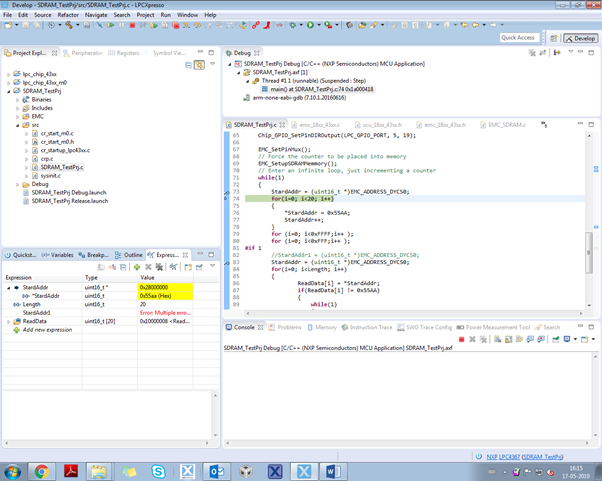
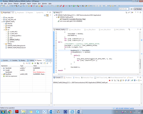
After loading the code I stop the code in while(1) , at "StardAddr = (uint16_t *)EMC_ADDRESS_DYCS0; "
here you can see that before initialization nothing is there in the expression. I have already written 0x55aa. so now it is expected that as I assign the address I should see the data 0x55aa l in the expression.
after running the code stepwise it is assigned and you can see the value as well in the expression side. Then i run the code and stop the debugger on the reading section
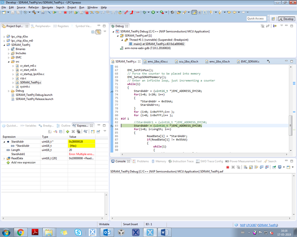
Here i am againg assigning the same variable pointer to the start of the SDRAM address. Now again if I asigned the address to the start location it is expected that it should show the same data again 0x55aa. but below you can see,
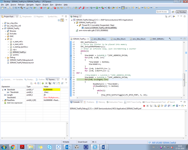
in the expression side no value is there even though the pointer is assigned to the SDRAM start addess 0x28000000. After running the code till ReadData[i] = *StardAddr1;
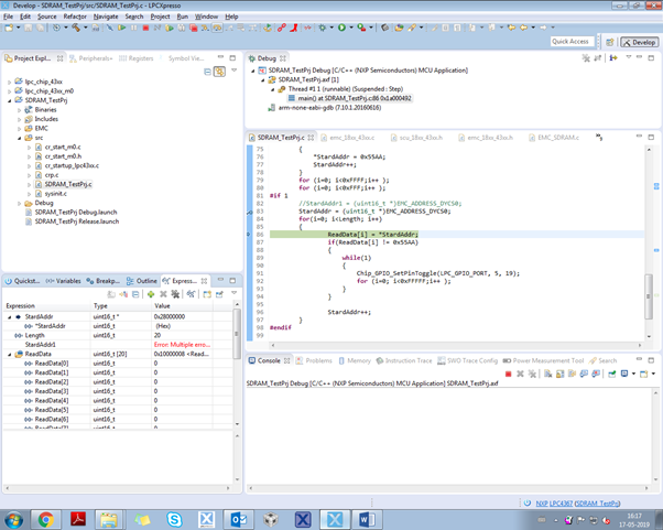
again step wise execution from the above line, it goes somewhere which cannot be traced,
Also it show in the expression side some error. Now I have terminate in order to come out of the loop. then it gives error as
"Target error from status-poll: Ee(FF). Redlink interface error 255."
I am not understanding the reason behind the same. is it a problem with the compiler or with SDRAM access routine?. I am using LPCXpresso IDE.
Refere the attached code as well.
NEed the solution for the same since it is required in the project ASAP.
Thanks
Gaurav More
- Mark as New
- Bookmark
- Subscribe
- Mute
- Subscribe to RSS Feed
- Permalink
- Report Inappropriate Content
Hi Gaurav More,
Thanks for your reply.
After reviewing the code carefully, I don't find the errors except that miss configuring the EMC_D7 pin, please check it.
Hope it helps.
Have a great day,
TIC
-------------------------------------------------------------------------------
Note:
- If this post answers your question, please click the "Mark Correct" button. Thank you!
- We are following threads for 7 weeks after the last post, later replies are ignored
Please open a new thread and refer to the closed one, if you have a related question at a later point in time.
-------------------------------------------------------------------------------
- Mark as New
- Bookmark
- Subscribe
- Mute
- Subscribe to RSS Feed
- Permalink
- Report Inappropriate Content
Hi Jeremy,
Thanks for the input. I missed the initialization of the EMC_D7. I made the modification in the code. I found that when i do debugging of the code it creates problem. But when i run without break points it it is running properly. This is say based on the the code I have written.
while(1)
{
Chip_GPIO_SetPinToggle(LPC_GPIO_PORT, 5, 19);
for (i=0; i<0xFFFFF;i++ );
StardAddr = (uint16_t *)EMC_ADDRESS_DYCS0;
for(i=0; i<20; i++)
{
*StardAddr = 0x55AA;
StardAddr++;
}
for (i=0; i<0xFFFF;i++ );
StardAddr = (uint16_t *)EMC_ADDRESS_DYCS0;
for(i=0; i<Length; i++)
{
ReadData[i] = *StardAddr;
if(ReadData[i] != 0x55AA)
{
while(1)
{
Chip_GPIO_SetPinState(LPC_GPIO_PORT, 5, 19, (bool) true);
}
}
StardAddr++;
}
for (i=0; i<0xFFFF;i++ );
return 0;
}/*Eof While*/
While running this code stepwise using debugging method it creates problem which I mentioned. But when I run the code without break point it runs and when it verifies the read and write data and if it proper then the LED will toggle and if there is a mismatch then the LED will be continuos ON.
This is how i am verifying the SDRAM read and write.
Reagarding the behaviour of the code is ther a problem if i debug the code with break points? Is this behaviour is correct?
I will also be working with NOR flash but the code available in the example codes mentioned that the NOR flash code is not tested.And the code is based on SPI flash not the parallel interface flash. I am lokking for paralle interface NOR Flash.
Do we have any sample code for reference w.r.t the interface of NOR flash?
Also can SDRAM and NOR FLash access is possible simultaneously?
It is required in our project on higher priority.
Thanks
Gaurav More
- Mark as New
- Bookmark
- Subscribe
- Mute
- Subscribe to RSS Feed
- Permalink
- Report Inappropriate Content
Hi Gaurav More,
Thanks for your reply.
Q1) Regarding the behavior of the code is the problem if I debug the code with breakpoints? Is this behavior is correct?
-- Yes, it's correct.
Q2) Do we have any sample code for reference w.r.t the interface of NOR flash?
-- No, however, in the periph_memtest demo, it's initialized the parallel flash, it's available to be testing as doing for the SDRAM.
/* Setup external memories */
void Board_SetupExtMemory(void)
{
/* Setup EMC Delays */
/* Move all clock delays together */
LPC_SCU->EMCDELAYCLK = ((CLK0_DELAY) | (CLK0_DELAY << 4) | (CLK0_DELAY << 8) | (CLK0_DELAY << 12));
/* Setup EMC Clock Divider for divide by 2 - this is done in both the CCU (clocking)
and CREG. For frequencies over 120MHz, a divider of 2 must be used. For frequencies
less than 120MHz, a divider of 1 or 2 is ok. */
Chip_Clock_EnableOpts(CLK_MX_EMC_DIV, true, true, 2);
LPC_CREG->CREG6 |= (1 << 16);
/* Enable EMC clock */
Chip_Clock_Enable(CLK_MX_EMC);
/* Init EMC Controller -Enable-LE mode */
Chip_EMC_Init(1, 0, 0);
/* Init EMC Dynamic Controller */
Chip_EMC_Dynamic_Init((IP_EMC_DYN_CONFIG_T *) &MT48LC4M32_config);
/* Init EMC Static Controller CS0 */
Chip_EMC_Static_Init((IP_EMC_STATIC_CONFIG_T *) &S29GL64N90_config);
/* Enable Buffer for External Flash */
LPC_EMC->STATICCONFIG0 |= 1 << 19;
}
Q3) Also can SDRAM and NOR flash access is possible simultaneously?
-- No, I'm afraid not.
Have a great day,
TIC
-------------------------------------------------------------------------------
Note:
- If this post answers your question, please click the "Mark Correct" button. Thank you!
- We are following threads for 7 weeks after the last post, later replies are ignored
Please open a new thread and refer to the closed one, if you have a related question at a later point in time.
-------------------------------------------------------------------------------
- Mark as New
- Bookmark
- Subscribe
- Mute
- Subscribe to RSS Feed
- Permalink
- Report Inappropriate Content
Hi Jeremy,
Any update regarding the SDRAM memory allocation using _SECTION and _DATA pragma mentioned above. I am checking but it is not reflectiong int he code as per the Placing data into different RAM blocks post.
As per the post i made the modification inthe code and added the following code.
__SECTION(data,RAM8) uint8_t data_buffer[1024];
uint8_t *StardAddr1;
uint16_t Length = 20;
uinsinged long i;
for (i=0;i<Length; i++)
{
data_buffer[i] = 0x0B;
}
while (1)
{
Chip_GPIO_SetPinToggle(LPC_GPIO_PORT, 5, 19);
for (i=0; i<0xFFFFF;i++ );
StardAddr1 = (uint8_t *)EMC_ADDRESS_DYCS0;
for (i=0;i<Length; i++)
{
if(data_buffer[i] != *StardAddr1)
{
Chip_GPIO_SetPinState(LPC_GPIO_PORT, 5, 19, (bool) true);
while(1) {}
}
}
}/* EOF While */
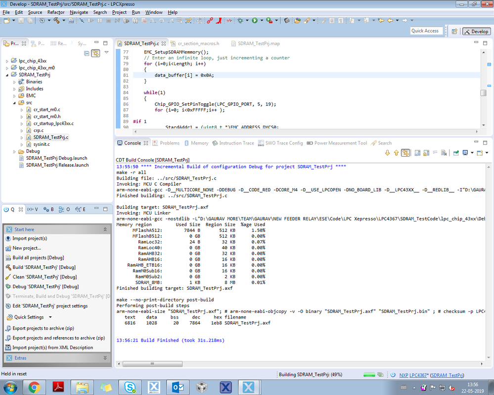
After compiling the code I got the data as menioned below
You can see that it is reflecting the memory as 1K used size.
but when I execute the following statement
for (i=0;i<Length; i++)
{
data_buffer[i] = 0x0B;
}
it is expected that it should only fill 20 locations instead of 1024. but while checking the code it fills all the location that is 1024.
StardAddr1 = (uint8_t *)EMC_ADDRESS_DYCS0;
for (i=0;i<Length; i++)
{
if(data_buffer[i] != *StardAddr1)
{
Chip_GPIO_SetPinState(LPC_GPIO_PORT, 5, 19, (bool) true);
while(1) {}
}
}
Here while executing the code while assigning the pointer to EMC_ADDRESS_DYCS0 and checking the expression it is visible that we can observe the value of *StardAddr1 which is the same as written in data_buffer. But it stuck in between since the length variable value is 2827 which is not the actual value.
Not able to figure out how it changes the values where i have assigne value 20 hardcoded.
All this issue comes while debugging and while free running menas removing the debugger and reseting the controller it works properly the LED toggling works fine,. So why is this ? since moving further it is required in the project that I need to used the debugging method to check the implementation with different variables allocated in different location.
Also now i am using __SECTION(data,RAM8) uint8_t data_buffer[1024]; This will place the 1024 byte buffer into the RAM8 but if i want another buffer to be allocated in the continuos memory location then shall I use below mentioned way?
__SECTION(data,(RAM8 + sizeof (data_buffer)) uint8_t data_buffer1[1024];
Please check the code I shared for that since I need to evaluation accessing time of SDRAM.
Thanks
Gaurav More
- Mark as New
- Bookmark
- Subscribe
- Mute
- Subscribe to RSS Feed
- Permalink
- Report Inappropriate Content
Hi Gaurav More
Thanks for your reply.
No doubt that the Placing data into different RAM blocks illustrate the correct way to place the data in the RAM,
And the key question is the data buffer[] array is capable of doing read and write operation or not, whether you give a try.
Have a great day,
TIC
-------------------------------------------------------------------------------
Note:
- If this post answers your question, please click the "Mark Correct" button. Thank you!
- We are following threads for 7 weeks after the last post, later replies are ignored
Please open a new thread and refer to the closed one, if you have a related question at a later point in time.
-------------------------------------------------------------------------------
- Mark as New
- Bookmark
- Subscribe
- Mute
- Subscribe to RSS Feed
- Permalink
- Report Inappropriate Content
Hi Jeremy,
I am able to allocate the data buffer array to SDRAM memory but when I am writing the data using
for (i=0;i<Length; i++)
{
data_buffer[i] = 0x0B;
}
This code and checking whether it is updated then it shows tha all the 1024 location is updated instead of 20 location. Why this is ? and
Also now i am using __SECTION(data,RAM8) uint8_t data_buffer[1024]; This will place the 1024 byte buffer into the RAM8 but if i want another buffer to be allocated in the continuos memory location then shall I use below mentioned way?
__SECTION(data,(RAM8 + sizeof (data_buffer)) uint8_t data_buffer1[1024];
Also please check the code where I have modified the EMCD7 pin configuration and also the allocation of the databuffer.
Thanks
Gaurav More
- Mark as New
- Bookmark
- Subscribe
- Mute
- Subscribe to RSS Feed
- Permalink
- Report Inappropriate Content
Hi Gaurav More
Thanks for your reply.
1) This code and checking whether it is updated then it shows that all the 1024 location is updated instead of 20 location. Why this is?
-- I'm not clear with your statement, please explain it.
2) Also now i am using __SECTION(data,RAM8) uint8_t data_buffer[1024]; This will place the 1024 byte buffer into the RAM8 but if i want another buffer to be allocated in the continuos memory location then shall I use below mentioned way?
-- Please refer to the thread Placing data at an address to make it.
3) Also please check the code where I have modified the EMCD7 pin configuration and also the allocation of the databuffer.
-- I already check it and it's correct now.
Have a great day,
TIC
-------------------------------------------------------------------------------
Note:
- If this post answers your question, please click the "Mark Correct" button. Thank you!
- We are following threads for 7 weeks after the last post, later replies are ignored
Please open a new thread and refer to the closed one, if you have a related question at a later point in time.
-------------------------------------------------------------------------------
- Mark as New
- Bookmark
- Subscribe
- Mute
- Subscribe to RSS Feed
- Permalink
- Report Inappropriate Content
Hi Jeremy,
1) This code and checking whether it is updated then it shows that all the 1024 location is updated instead of 20 location. Why this is?
--- I declared the uint8_t data_buffer arrary of size 1024 bytes. Now I have assigned the data_buffer to SDRAM location using __SECTION(data,RAM8) uint8_t data_buffer[1024];
Now in main I am only filling 20 array location with 0x0B using where Length = 20
for (i=0;i<Length; i++)
{
data_buffer[i] = 0x0B;
}
But after completion of the loop I found that all 1024 array is filled with 0x0B. It is expected that only from data_buffer[0] to data_buffer[19], it should fill 0x0B rest all should be 0. This is what is happening and I am not understanding the reason for the same.
Also in addition although it is filled with 1024 array with oxoB, I moved forward to check whether the value is fillled at the SDRAM location where the data_buffer is allocated using another pointer .
uint8_t *StardAddr1;
StardAddr1 = (uint8_t *)EMC_ADDRESS_DYCS0;//0x28000000
for (i=0;i<Length; i++)
{
if(data_buffer[i] != *StardAddr1)
{
Chip_GPIO_SetPinState(LPC_GPIO_PORT, 5, 19, (bool) true);
while(1) {}
}
}
Now Length variable value is 20. So it means it should check only 20 array locations but when I check in debug mode the value of length variable is something 2527. So iIam not understanding this behaviour and also in that case if I check in debug mode then the debugger hangs and then only way is to terminate it and again reload. but when I remove the debugger and reset the board then the code works properply as per the LED indication.
Now there is confusion that even though the code is working fine in free running mode, is it checking only for 20 array location out of 1024?
Over all it is difficult to understand the behaviour of the debbuger and that why I ask you to check the modified code where whether i have made any mistake or missing any modification which is affecting the debugging of the code?
Is there any issue with the debugger when executing the external RAM code access?
Also one more question:
Do we have an sample code for NOR flash interface with any other controll apart from LPC4367?
Need for the reference and validation.
Thanks
Gaurav More
- Mark as New
- Bookmark
- Subscribe
- Mute
- Subscribe to RSS Feed
- Permalink
- Report Inappropriate Content
Hi Jeremy,
Thanks for your reply. I will check with the code for NOR flash and get back to you. Before that I am trying to allocate the memory to the buffer. for that i referedPlacing data into different RAM blocks thread. But still no success.
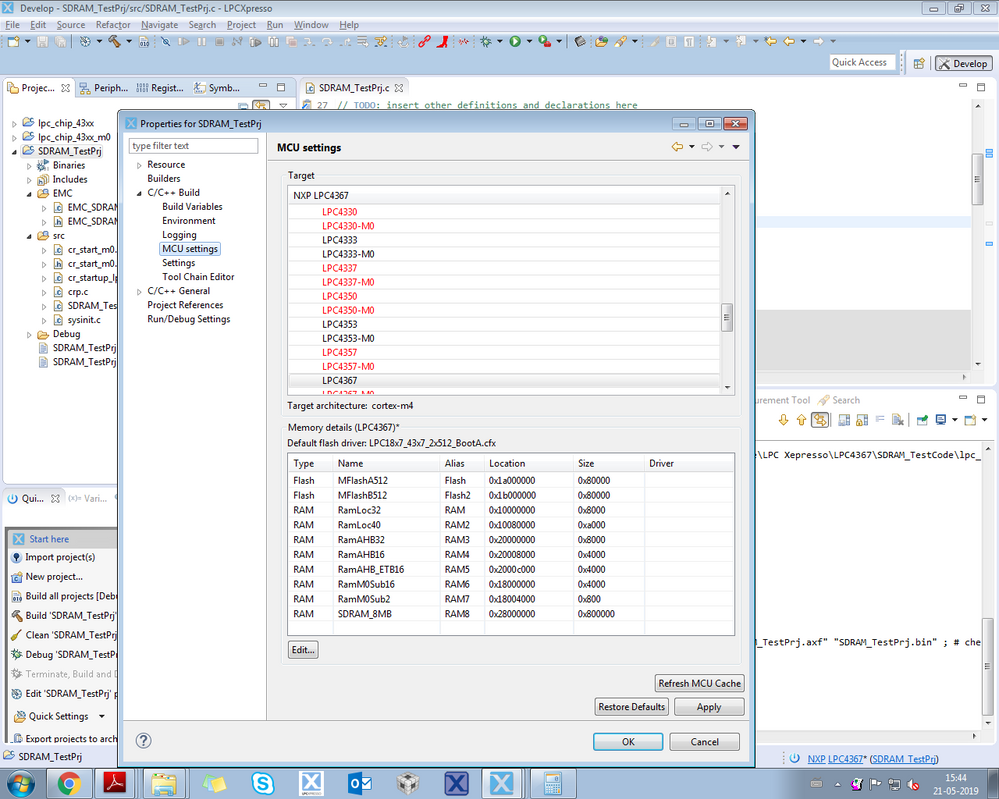
I created the memory in MCU setting as SDRAM_8MB
Then using _DATA(RAM) I allocated the buffer
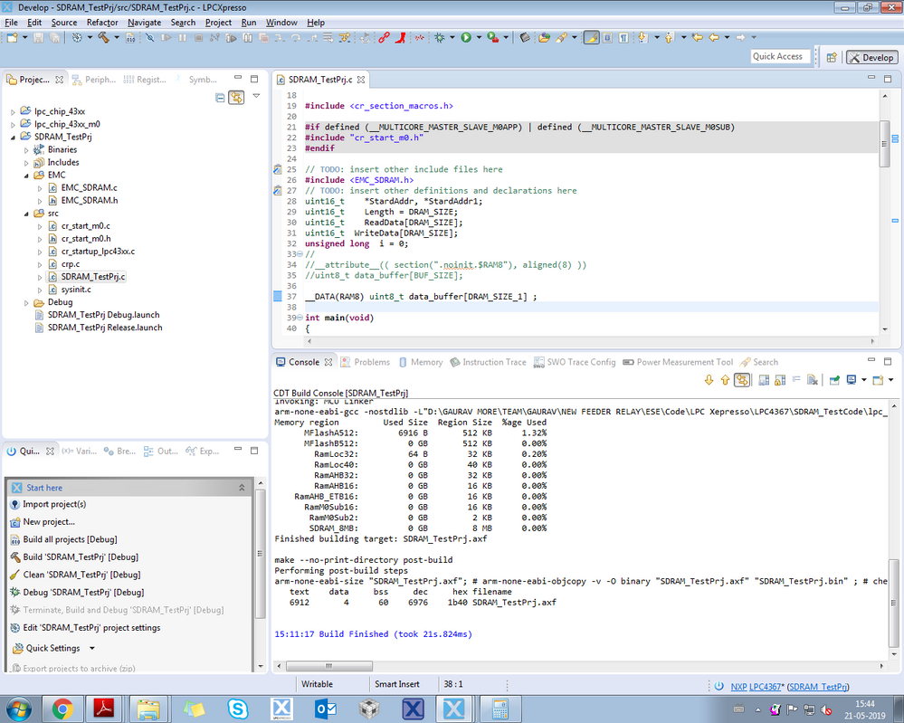
__DATA(RAM8) uint8_t data_buffer[DRAM_SIZE_1] ; then after compilation it was not showing the correct values as shown below you can see that the memory size and name exisit but used size is 0 where it should be 1KB
I have attached the Code for your reference. Kindly check for the same. I also check .Map file but still it did not show the variable name which i used. Also tried to use.
__attribute__(( section(".noinit.$RAM5"), aligned(8) ))
uint8_t data_buffer[BUF_SIZE];
But again no success. Output is same as above. Please check the code and let me know since im using LPCXpresso so the mehtod are different and i am trying those methods only. Please check the code meanwhile i will refer the forums for the same to check whether there is any mistake from my side in the code.
Thanks
Gaurav More.
