
- NXP Forums
- Product Forums
- General Purpose MicrocontrollersGeneral Purpose Microcontrollers
- i.MX Forumsi.MX Forums
- QorIQ Processing PlatformsQorIQ Processing Platforms
- Identification and SecurityIdentification and Security
- Power ManagementPower Management
- MCX Microcontrollers
- S32G
- S32K
- S32V
- MPC5xxx
- Other NXP Products
- Wireless Connectivity
- S12 / MagniV Microcontrollers
- Powertrain and Electrification Analog Drivers
- Sensors
- Vybrid Processors
- Digital Signal Controllers
- 8-bit Microcontrollers
- ColdFire/68K Microcontrollers and Processors
- PowerQUICC Processors
- OSBDM and TBDML
-
- Solution Forums
- Software Forums
- MCUXpresso Software and ToolsMCUXpresso Software and Tools
- CodeWarriorCodeWarrior
- MQX Software SolutionsMQX Software Solutions
- Model-Based Design Toolbox (MBDT)Model-Based Design Toolbox (MBDT)
- FreeMASTER
- eIQ Machine Learning Software
- Embedded Software and Tools Clinic
- S32 SDK
- S32 Design Studio
- Vigiles
- GUI Guider
- Zephyr Project
- Voice Technology
- Application Software Packs
- Secure Provisioning SDK (SPSDK)
- Processor Expert Software
-
- Topics
- Mobile Robotics - Drones and RoversMobile Robotics - Drones and Rovers
- NXP Training ContentNXP Training Content
- University ProgramsUniversity Programs
- Rapid IoT
- NXP Designs
- SafeAssure-Community
- OSS Security & Maintenance
- Using Our Community
-
-
- Home
- :
- Topics
- :
- NXP Designs Knowledge Base
- :
- Homebrew RF Design Challenge Winners
Homebrew RF Design Challenge Winners
- Subscribe to RSS Feed
- Mark as New
- Mark as Read
- Bookmark
- Subscribe
- Printer Friendly Page
- Report Inappropriate Content
Homebrew RF Design Challenge Winners
Homebrew RF Design Challenge Winners

Description
Earlier this year NXP organized a promotional opportunity for amateur radio enthusiasts to use their creativity and build their own power amplifier designs.
NXP received numerous creative submissions in this competitive Homebrew RF Design Challenge. We appreciate the dedication and enthusiasm from the community that made this contest a success.
First place winner
An MRF101AN broadband amplifier design with 1 W Input, 100 W Output 1.8-54 MHZ Amplifier deck. (For more information visit:NXP MRF-101 - RFPowerTools )

It is an amplifier with a bandwidth of 1.8MHz to 54MHz. Maximum output power of 100W up to 30MHz and 70W up to 50MHz.
Maximum power supply 50V to 4A, with a Voltage Standing Wave Ratio of 1.5:1 maximum.
The design dimensions of the PCB is 5x5 cm (2x2 in). and 310g weight including fan and heat sink.
Second place winner
A 600W broadband HF amplifier using affordable LDMOS devices (For more information visit: https://qrpblog.com/2019/10/a-600w-broadband-hf-amplifier-using-affordable-ldmos-devices/ )
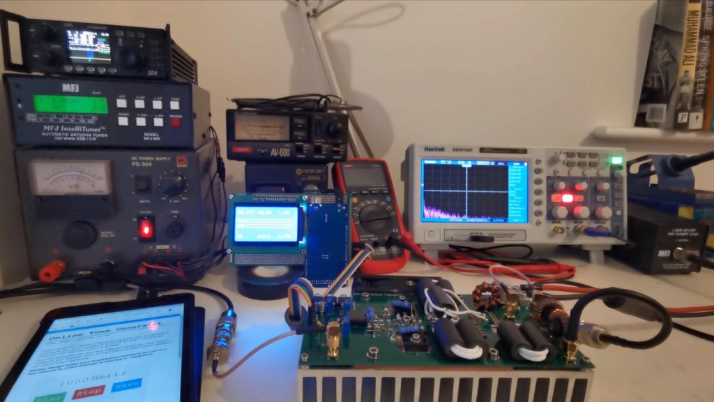
This project is meant to demonstrate the capabilities of the MRF300 transistors as linear broadband devices in the 2-50MHz range and to be used by radio amateurs as a starting point for a medium-high power amplifier. This is also my entry to the NXP Homebrew RF Design Challenge 2019.
To achieve the target of 600W output while also minimizing the level of even-number harmonics, a “push-pull” configuration of two transistors is used. Luckily, the manufacturer made it easy to design the PCB layout for such a thing by offering two versions (the MRF300AN & MRF300BN) that have mirrored pinout. The common TO-247 package is used, with the source connected to the tab.
Each individual MRF300 LDMOS transistor is specified at 330W output over a 1.8-250MHz working frequency range, a maximum 28dB of gain and over 70% efficiency. The recommended supply range is 30-50Vdc. By studying the specifications, it looks like with correct broadband matching and some operational safety margin we can get close to 600W output at a voltage of around 45V across a resonably large bandwidth; the aim is to cover 1.8 to 54MHz.
Main challenges when designing this amplifier are related to achieving good input and output matching over the entire frequency range as well as maintaining high and flat gain. Good linearity and a low level of harmonic products are mandatory. As the TO-247 is not a package specifically designed for high-power RF, there are some challenges with thermal design and PCB layout as well.
Information taken from the essay by the winner.
Third place winner
A High Efficiency Switchmode RF Amplifier using a MRF101AN LDMOS Device for a CubeSat Plasma Thruster (For more information visit: Research - SuperLab@Stanford )


The Class E amplifier utilizes the active device as a switch, operating in only cutoff (off) and saturated (on) conditions. This minimizes the overlap of voltage and current, reducing losses in the active device. To further reduce loss the Class E amplifier utilizes an inductively tuned resonant network to achieve zero voltage switching, bringing the voltage across the switch to zero before turn on, eliminating energy stored in the output capacitance of the active device that would otherwise be dissipated. This is achieved with an inductively tuned series resonant output filter.
In the Class E amplifier losses are almost entirely determined by the current conducted by the active device so a high drain impedance is desired to maximize efficiency. The drain impedance is ultimately limited by the voltage rating of the switch. For our desired output power of 40W and the maximum voltage rating of 133V for the MRF101AN this impedance is still less than 50 ohms, so a L match circuit is used to match the drain impedance to 50 ohms. The load network in our design provides a drain impedance of 15.4+12.8j.
As the MRF101AN will operate in saturation a high drive level is desired. To eliminate the need for a preamplifier and allow for digital control, we use a high speed gate drive chip typically used in switch-mode power supplies, LMG1020, to drive the MRF101AN instead of a RF preamplifier. A resonant network is used to provide voltage gain at the fundamental and third harmonic, providing a quasi-square wave on the gate which helps insure the device remains in saturation.
Conclusion
It was a close call and highly competitive! Each participant had their own creative, unique and impressive way of displaying the capabilities of these new parts.
NXP is always up for new design challenges.
Ready for the next challenge?