- NXP Forums
- Product Forums
- General Purpose MicrocontrollersGeneral Purpose Microcontrollers
- i.MX Forumsi.MX Forums
- QorIQ Processing PlatformsQorIQ Processing Platforms
- Identification and SecurityIdentification and Security
- Power ManagementPower Management
- MCX Microcontrollers
- S32G
- S32K
- S32V
- MPC5xxx
- Other NXP Products
- Wireless Connectivity
- S12 / MagniV Microcontrollers
- Powertrain and Electrification Analog Drivers
- Sensors
- Vybrid Processors
- Digital Signal Controllers
- 8-bit Microcontrollers
- ColdFire/68K Microcontrollers and Processors
- PowerQUICC Processors
- OSBDM and TBDML
-
- Solution Forums
- Software Forums
- MCUXpresso Software and ToolsMCUXpresso Software and Tools
- CodeWarriorCodeWarrior
- MQX Software SolutionsMQX Software Solutions
- Model-Based Design Toolbox (MBDT)Model-Based Design Toolbox (MBDT)
- FreeMASTER
- eIQ Machine Learning Software
- Embedded Software and Tools Clinic
- S32 SDK
- S32 Design Studio
- Vigiles
- GUI Guider
- Zephyr Project
- Voice Technology
- Application Software Packs
- Secure Provisioning SDK (SPSDK)
- Processor Expert Software
-
- Topics
- Mobile Robotics - Drones and RoversMobile Robotics - Drones and Rovers
- NXP Training ContentNXP Training Content
- University ProgramsUniversity Programs
- Rapid IoT
- NXP Designs
- SafeAssure-Community
- OSS Security & Maintenance
- Using Our Community
-
-
- Home
- :
- General Purpose Microcontrollers
- :
- Kinetis Microcontrollers Knowledge Base
- :
- UART Emulation Using the FTM or TPM
UART Emulation Using the FTM or TPM
- Subscribe to RSS Feed
- Mark as New
- Mark as Read
- Bookmark
- Subscribe
- Printer Friendly Page
- Report Inappropriate Content
UART Emulation Using the FTM or TPM
UART Emulation Using the FTM or TPM
Introduction
Even with the prevalence of universal asynchronous receiver/transmitter (UART) peripherals on microcontrollers (MCUs), bit banged UART algorithms are still used. The reasons for this vary from application to application. Sometimes it is simply because more UARTs are needed than the selected device provides. Maybe application or layout restrictions require certain pins to be used for the UART functions but the device does not route UART pins to the required package pins. Maybe the application requires a non-standard or proprietary UART scheme.
Whatever the reason, there are applications where a bit banged UART is used and is typically a pure software implementation (a timer is used and the MCU core controls a GPIO pin directly). A better alternative may be to use Flextimer (FTM) or Timer/PWM Module (TPM) to take advantage of the features of these peripherals and possibly offload the CPU. This document will explain and provide a sample application of how to emulate a UART using the FTM or TPM peripheral. A Kinetis SDK example (for the TWR-K22F120M and FRDM-K22F platforms) and a baremetal legacy code example (for the FRDM-KL26Z) are provided here.
UART protocol
Before creating an application to emulate a UART, the UART protocol and encoding must be understood. The UART protocol is an asynchronous protocol that typically includes a start bit, payload (of 7-10 data bits), and a stop bit but does allow for many variations on the number of stop bits and what/how to transfer the data. For this document and application example, the focus will be UART transmission that follows 1 start bit, 8 data bits, 1 stop bit, no parity, and no flow control. The data will be transmitted least significant bit (LSB) first. The following image is a block diagram of this transmission.
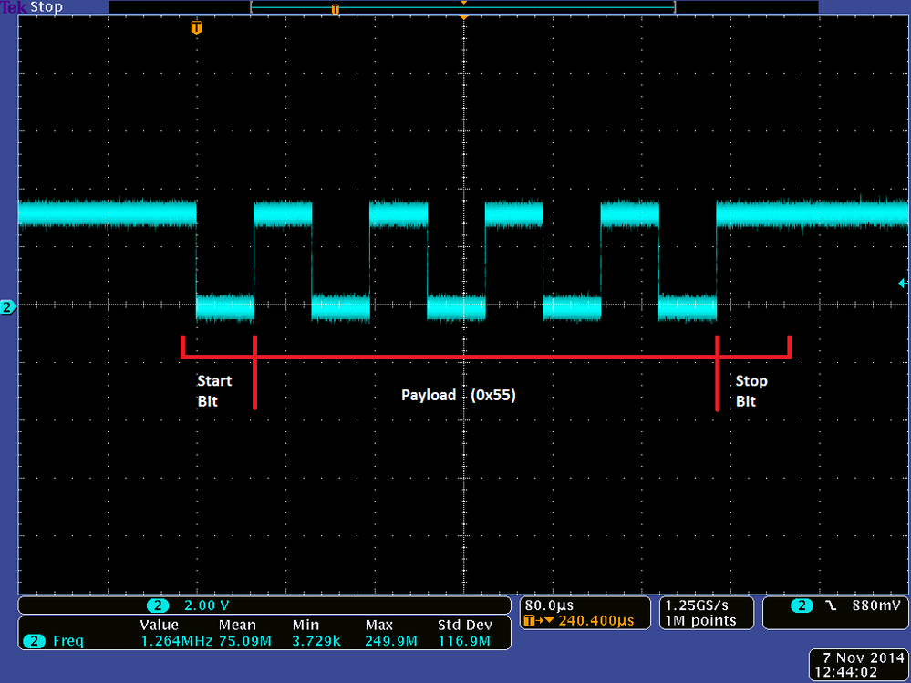
However, this doesn't specify what the transmission looks like electrically. The figure below shows a screenshot of an oscilloscope capture of a UART transmission. The data transmitted is 0x55 or a "U" in the ASCII representation.
Notice that the transmission line is initially a logic high, and then transitions low to signal the start of the transmission. The transmission line must stay low for one bit width for the receiver to detect it. Then there are 8 data bits, followed by 1 stop bit. In the case shown above, the data bits are 0x55 or 0b0101_0101. Remember that the transmissions are sent LSB first, so the screenshot shows 1-0-1-0-1-0-1-0. The last transition high marks the beginning of the stop bit and the line remains in that state until the start of the next transmission. The receiver, being asynchronous, does not require any type of identifying transition to mark the end of the stop bit.
FTM/TPM configuration
The first question many may ask when beginning a project like this is "How do I configure the FTM/TPM when emulating a UART". The answer to this depends on the aspect of this problem you are trying to solve. Transmitting and receiving characters require two different configurations. Transmission requires a configuration that manipulates the output pin at specific points in time. Receiving characters requires a configuration that samples the receive pin and measures the time between pin transitions. The FTM and TPM have the modes listed in the following table:
The FTM and TPM have four different modes that manipulate an output: Output compare (no pulse), Output compare (with pulse), Edge-aligned PWM, and Center-aligned PWM. Neither PWM mode is ideal for the requirements of the application. This is because the PWM modes are designed to produce a continuous waveform and are always going to return to the initialized state once during the cycle of the waveform. However, the UART protocol may have continuous 1's or 0's in the data without pin transitions between them.
The output compare mode (high-true or low-true pulse modes) is designed to only manipulate the pin once, and only produces pulses that are one FTM/TPM clock cycle in duration. So this is obviously not desirable for the application. The output compare mode (Set/Clear/Toggle on match) is promising. This mode manipulates the output pin every cycle. There are three different options: clear output on match, set output on match, and toggle output on match. Neither "clear output on match" nor "set output on match" are ideal as either would require configuration changes during the transmission of a character. The "toggle output on match", however, can be used and is the selected configuration mode for this sample application.
To receive characters, there is only one mode that is intuitive: "the input capture mode". This mode records the timer count value on an edge transition of the selected input pin. Similar to the output compare mode chosen for the transmit functionality, the input capture mode has three sub-modes: capture on rising edge, capture of falling edge, and capture on either edge. It is clear from the descriptions that capture on either edge should be selected.
Transmit encoding
The selection of the FTM/TPM mode is moderately intuitive, but using this mode to emulate a UART transmission is not. There are two issues that make this a little tricky.
1) The output pin is initialized low. However, the UART protocol needs the pin to begin in a logical high state.
2) The pin transitions on every cycle provided the channel value is less than the value of the MOD register. Due to continuous strings of 1's or 0's, it is necessary to have periods where the pin does not transition.
Both of these points have workarounds.
Output pin initialization
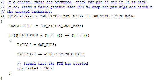
For the first issue, the channel interrupt is first enabled and the channel value register is loaded with a value much less than the value in the MOD register. Then in the channel interrupt service routine, the pin is sampled to ensure that it is in the logic high state and the channel interrupt is disabled (and will not be re-enabled throughout the life of the application). The code for this interrupt service routine is as follows.
Output pin control
For the second issue, a method of not transitioning the pin value while allowing the timer to continue counting normally is necessary. The Output Compare mode uses the channel value register to determine when the pin transition occurs. If a value greater than MOD is written to the channel value register, the channel value will never match the count register and thus, a pin transition will never occur. So, when a series of continuous 1's or 0's need to be transmitted, a value greater than the value in the MOD register can be written to the channel value register to keep the output pin in its current state. However, when a value greater than MOD is written to the channel value register, no channel match will occur (which means channel interrupts will not occur). So the timer overflow interrupt must be used to continue writing values. This requires the updates to be output pin to be planned ahead of time and makes the transmission algorithm a little tricky. The following diagram displays when which values should be written to the channel value register at which points in time to generate the appropriate pulses.
Writing a function to translate a number into the appropriate series of MOD/2 and MOD+1 values can be a little tricky. To do this, we must first notice that MOD/2 needs to be written when changes on the transmission pin are need and MOD+1 needs to be written when pin transmissions are not desired. So, what logical function can we use to determine when a change has happened? XOR is the correct answer. So what two values need to be XOR'd together? One value is obviously the value that we want to send. But what is the second value? It turns out that the second value is a shifted version of the value that we want to send. Specifically, the second value is the desired value to send shifted to the left by one. (You can think of it as sort of a "future" value of the desired value). The following pictures show how to determine the queue to use for the transmission.
Receive decoding
The receive functionality has an advantage over the transmit functions in that it is possible to use DMA for the reception of characters. This is because the receive function takes advantage of the input capture functionality of the FTM / TPM and therefore can use the channel match interrupt. The example application provided with this document implements a DMA method and a non-DMA method for reception. First, the non-DMA method will be discussed. Before discussing the specifics of gathering the input pulse widths, some details of the receive pin need to be discussed.
Detecting the start bit
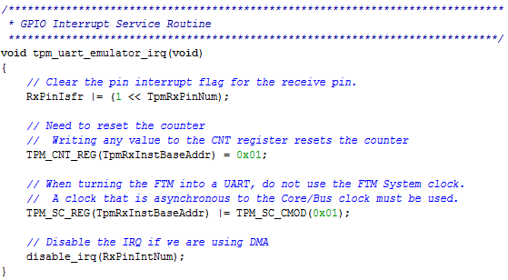
The receive pin needs to be able to determine when the start of the packet transmission begins. To do this, the receive pin is configured as an FTM / TPM pin. At the same time, the GPIO interrupt functionality is configured on the same pin for a falling edge interrupt. The GPIO interrupt capabilities are enabled in any digital mode, so the GPIO interrupt will still be able to be routed to the Nested Vector Interrupt Controller (NVIC). The pin interrupt is used to start the FTM / TPM clock when a new character reception begins. In the GPIO interrupt for this pin, the FTM / TPM counter register is reset and the clock to the FTM / TPM is turned on. The code for the GPIO interrupt service routine is shown below.
Receiving characters without DMA
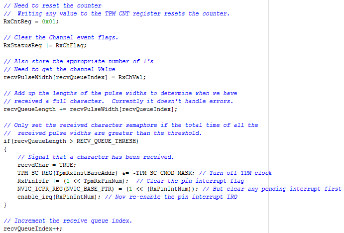
Now, when receiving characters and not using DMA, the first thing to understand is that the Interrupt Service Routine (ISR) will be used and it will mainly be used to record the captured count values. The interrupt service routine also tracks the current receive character length and resets the counter register. This is so that the values in the receive queue reflect the time since the last pin transition. The interrupt function for the non-DMA application is shown below.
Notice that the first two actions in the ISR are resetting the count register, and clearing the channel event interrupt flag. Then the channel value is stored in the receive pulse width array (this is simply an array that holds the receive pulse widths of the current character being received). Next, recvQueueLength, the variable which holds the current length of the character being received, is updated to reflect the latest character length. The next step is to determine if the full character has been received. This is determined by comparing recvQueueLength to the RECV_QUEUE_THRESH, which is the threshold as determined by multiplying the number of expected bits by the expected bit width plus another bit width (for the start bit). If the recvQueueLength is greater than the RECV_QUEUE_THRESH, then a semaphore is set, recvdChar, to indicate that a full character has been received. The FTM / TPM clock is turned off, and the pin interrupt functionality of the receive pin is enabled. The final step in the interrupt routine is to increment the receive queue index, recvQueueIndex. This variable points to the current entry in the receive queue array.
Using DMA to receive characters
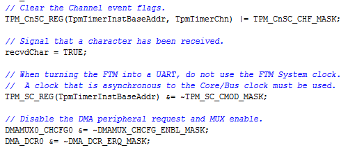
When using DMA, the receive FTM / TPM interrupt is much different. The interrupt routine simply needs to clear the channel interrupt flag, stop the FTM / TPM timer, disable the DMA channel, and set the received character semaphore. The character is then decoded outside of the interrupt routine. The interrupt function when using DMA is shown below:
Decoding the received pulse widths
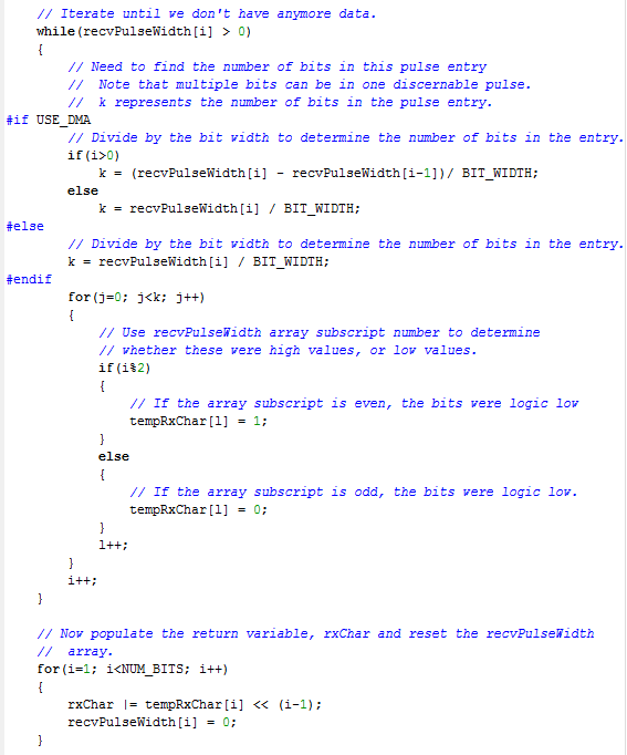
Once the array of pulse widths has been populated, the received character needs to be translated into a single number. This varies slightly when using DMA and when not using DMA. However, the basic principle is the same. The number of bits in a single entry is determined by dividing by the expected bit width and this is translated into a temporary array that contains 1's and 0's, and then that is used to shift in the appropriate number of 1's and 0's into the returned char variable. A temporary array is needed because the values are shifted into the UART LSB first, so the bit must be physically flipped from the first entry to the last. There is no logical operation that will do this automatically. The algorithm to perform this translation is shown below. In this algorithm, note that recvPulseWidth is the array that contains the raw count value of the pulse width. The array tempRxChar holds the decoded character in reverse order and rxChar is a char variable that holds the received character.
Conclusion
This document provides an overview of the UART protocol and describes a method for creating a software UART using the timing features of the FTM or TPM peripheral. This method allows for accurate timing and while not relying entirely on the CPU and the latency associated with the interrupt and the GPIO pins. The receive function is open to further optimization by using DMA, which can provide further unloading of the CPU.

